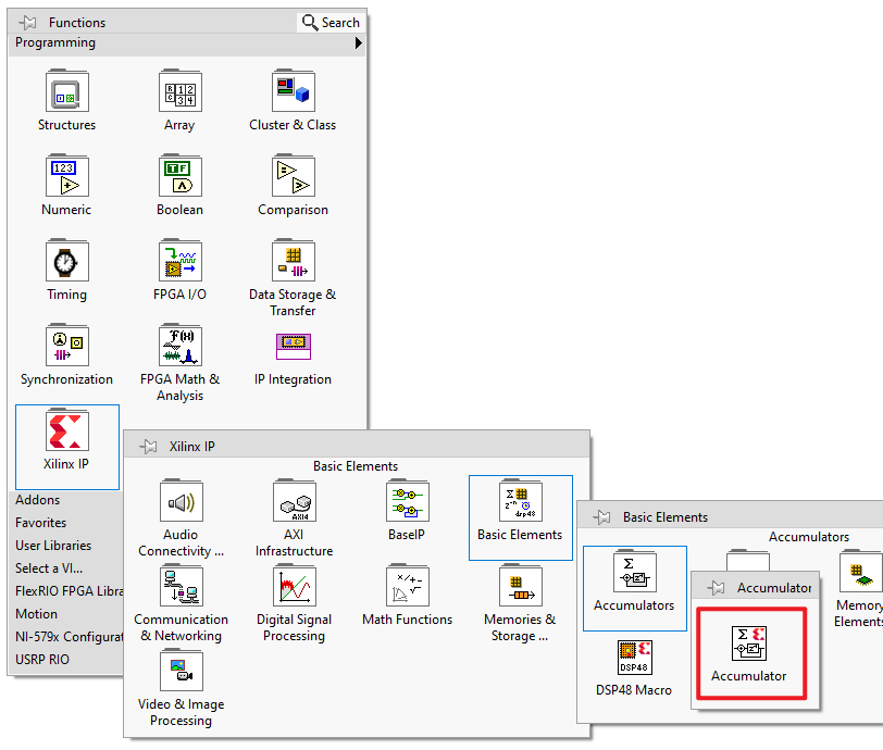
1. The IP locates in:
Functions/Programming/Xilinx IP/Basic Elements/Accumulators/Accumulator (as shown below)
2. Double click the original IP node to open LabVIEW configuration window of it.
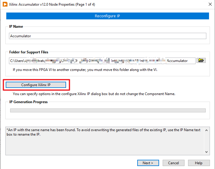
3. Click
Configure Xilinx IP button to open Vivado customize IP window.
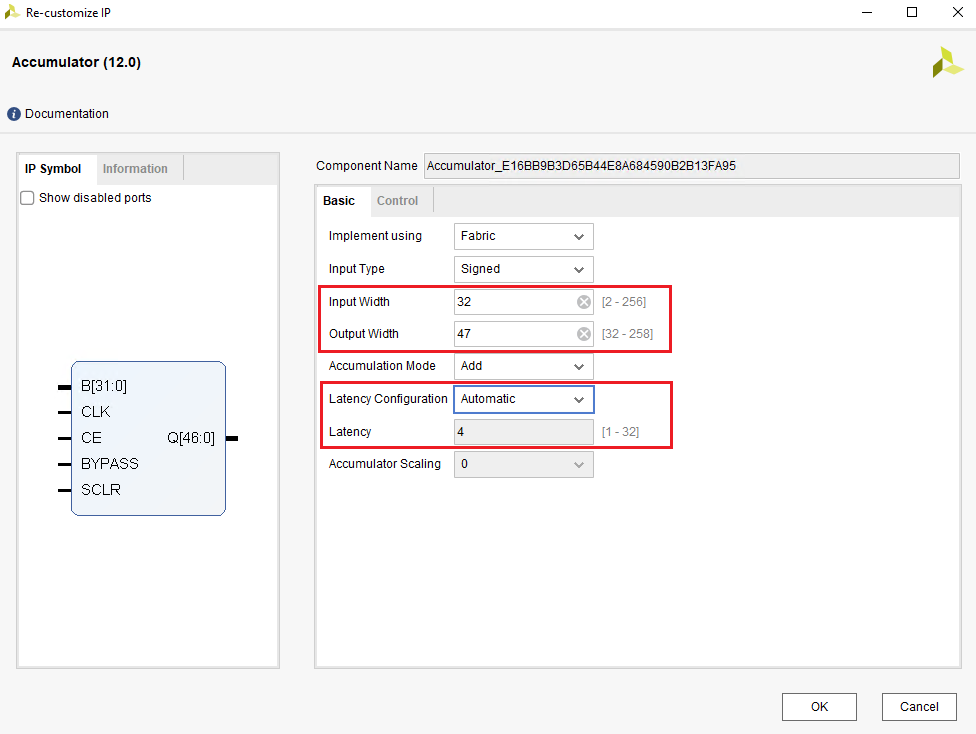
a. Set the Input Width based on your need;
b. Set the Output Width based on your need;
c. Configure Latency, if you choose the latency as
Automatic, you can see the Vivado calculate the actual Latency for you, shown in an indicator.
4. Enable
Clock Enable(CE), this is an enable input for IP to use the source clock. This input is critical, since in FPGA, the valid data will not always be ready on each clock tick. You can wire a FIFO's
output valid boolean to
CE to well control IP's behavior.
5. Enable
Synchronous Clear (SCLR), this is an reset input for IP to clear current register and set back to
0. If you would like to have a custom initial value, you can use
Synchronous Init (SINIT).
6.
Optional: Enable
Bypass and select
Active Low/Active High for this input.
If
Bypass is active, the IP pass the input(B) it received directly to output(Q).
If
Bypass is inactive, the IP execute accumulation work, and output(Q) the accumulation answer.
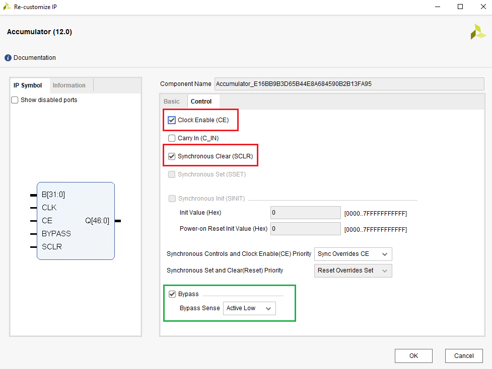
7. Click OK, Vivado will generate the IP for you.
8. After IP Generation Progress completed its work, click next to configure the IP's LabVIEW interface.
a. enable the clock signal, and other IP Enable Signal(s) you need. Ex. CE, BYPASS, SCLR.
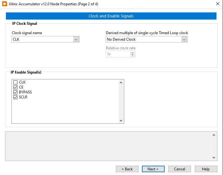
b. Click next, and go to IP Terminals Page.
Here, you need to define your terminals data type in LabVIEW.
Make sure the length of B & Q are the same as which you set in Vivado (Step 3), and set the
Integer word Length.
If you would like to keep the precision of input and output to be the same, just let the
Length -
Integer word Length to be equivalent. Ex ( 32-5 = 47-20 in the below picture)
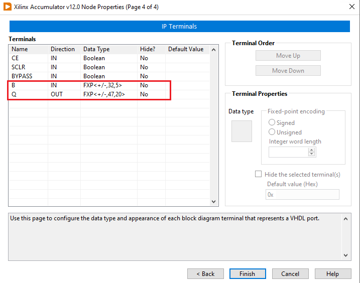
9. Click
Finish, and wire the IP with other components in your FPGA vi.
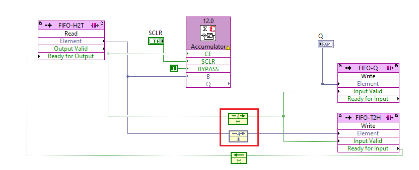
Pay attention to the latency property of the IP.
A valid output will be generated after it accepts a valid input with
latency clock ticks.
In my case, Latency is 4. So, I need to give 4 period delay on the valid control signal.