Configuring Component-Level IP (CLIP)
Several CLIPs are installed along with the X410 Reference Project. These CLIPs can be found here:
..\LabVIEW xxxx\Targets\NI\FPGA\USRP\X410\CLIP
For a 1 SPC configuration, use the RF2x2_100M_CLIP
For a 4 SPC configuration, use the RF2x2_400M_CLIP
To add a CLIP, right-click on the FPGA (USRP-X410) Target in the Reference project and choose Properties >> Component-Level IP
Use the + icon to browse and add the needed CLIP.

Once a new CLIP has been added to the project, right-click on the Daughterboard nodes in the project to select the CLIP declaration.

Conditional Disable Symbols
The Reference projects contain several Conditional Disable Symbols.
To configure these, right-click on the FPGA (USRP-X410) Target in the Reference project and choose Properties >> Conditional Disable Symbols

|
Conditional Disable Symbol
|
Description
|
Default
value
|
Used by NI-USRP
|
|
ACQ_PATH
|
If enabled, DSP will be performed on acquired data (RX)
|
ENABLED
|
|
|
ACQ_DIGITAL_OFFSET
|
Enable/Disable Digital Offset DSP on RX path
|
ENABLED
|
No
|
|
ACQ_DIGITAL_GAIN
|
Enable/Disable Digital Gain DSP on RX path
|
ENABLED
|
No
|
|
ACQ_EQUALIZATION
|
Enable/Disable Equalization DSP on RX path
|
DISABLED
|
No
|
|
ACQ_FREQUENCY_SHIFT
|
Enable/Disable Frequency Shift DSP on RX path
|
ENABLED
|
Yes
|
|
ACQ_IQ_IMPAIRMENTS
|
Enable/Disable Digital Offset DSP on RX path
|
ENABLED
|
No
|
|
ACQ_DECIMATION
|
Enable/Disable Digital Offset DSP on RX path
|
FRACTIONAL
|
Yes
|
|
ACQ_SYNC
|
Enable/Disable Sync Trigger on RX path
|
ENABLED
|
Yes
|
|
GEN_PATH
|
If enabled, DSP will be performed on generated data (TX)
|
ENABLED
|
|
|
GEN_DIGITAL_OFFSET
|
Enable/Disable Digital Offset DSP on TX path
|
ENABLED
|
No
|
|
GEN_DIGITAL_GAIN_PRE
|
Enable/Disable Digital Pre Gain DSP on TX path
|
ENABLED
|
No
|
|
GEN_EQUALIZATION
|
Enable/Disable Equalization DSP on TX path
|
DISABLED
|
No
|
|
GEN_FREQUENCY_SHIFT
|
Enable/Disable Frequency Shift DSP on TX path
|
ENABLED
|
Yes
|
|
GEN_IQ_IMPAIRMENTS
|
Enable/Disable IQ Impairments DSP on TX path
|
ENABLED
|
No
|
|
GEN_INTERPOLATION
|
Enable/Disable Interpolation DSP on TX path
|
FRACTIONAL
|
Yes
|
|
GEN_DIGITAL_GAIN_POST
|
Enable/Disable Digital Post Gain DSP on TX path
|
ENABLED
|
No
|
|
GEN_SYNC
|
Enable/Disable Sync Trigger on TX path
|
ENABLED
|
|
|
ACQ_NUM_CHANNELS
|
Number of acquisition channels (RX)
|
|
|
|
GEN_NUM_CHANNELS
|
Number of generation channels (TX)
|
|
|
|
ACQ_GEN_SPC
|
Number of Samples Per Cycle (1 or 4)
|
|
|
|
FPGA_EMULATION
|
Enable FPGA Emulation in the Register Bus
|
|
|
|
FPGA_TARGET_CLASS
|
URSP_X410 or USRP_X410_EMBEDDED
|
|
|
Table of Conditional Disable Symbols used in the Reference FPGA project
Loading a bitfile
Use the following Open Session VIs to load a specific bitfile created by the Reference FPGA project.
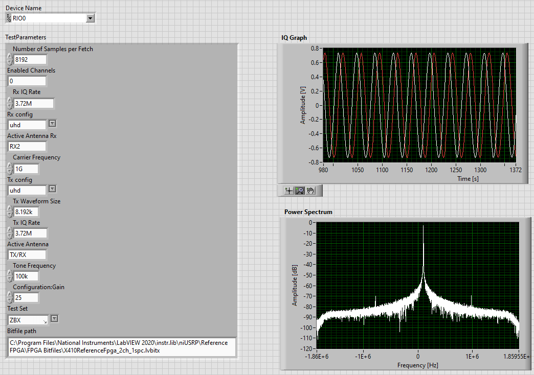
Below is an example of a desktop VI that loads a specific bitfile and starts generation and acquisition of the IQ data.
Note: this VI is not included in the example files. Users need to recreate it.


-
In this example, note that both Rx config and Tx config are set to none. The niUSRP Open Rx Session with Custom Bitfile.vi allows you to specify that in this case, we are not using the driver for Rx and Tx front-end configuration. This test VI runs a bitfile set up for internal loopback between Tx and Rx on the FPGA:
-

..instr.lib\niUSRP\Reference FPGA\Reference FPGA X410 Debug.vi
This allows you to use the NI-USRP driver to set up and configure parts of the system while you are responsible in this case for the Tx and Rx portion. Similarly, you can disable streaming and implement that locally on the FPGA.
Using the RIO interface
It is possible to open an FPGA VI Reference in addition to using the niUSRP Open. This allows you to use the Read/Write Control to read or write to Front Panel controls on your main FPGA VI. See the example below.
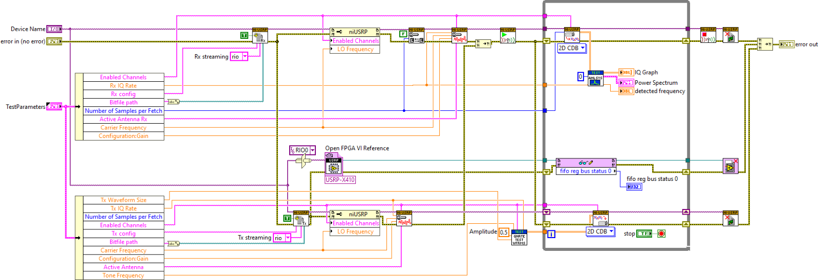
This is a very useful technique for adding debug information to your FPGA VI. Note that the Open FPGA VI Reference must use the same bitfile that is used by the niUSRP Open and that you can not use the download method on the RIO session while a niUSRP session is open.
Using niUSRP_SetAttribute.vi to directly control DSP
This utility VI allows you to directly set attributes in the ni-usrp driver:
C:\Program Files\National Instruments\LabVIEW <Version>\instr.lib\niUSRP\niUSRP Set Attribute (DBL).vi
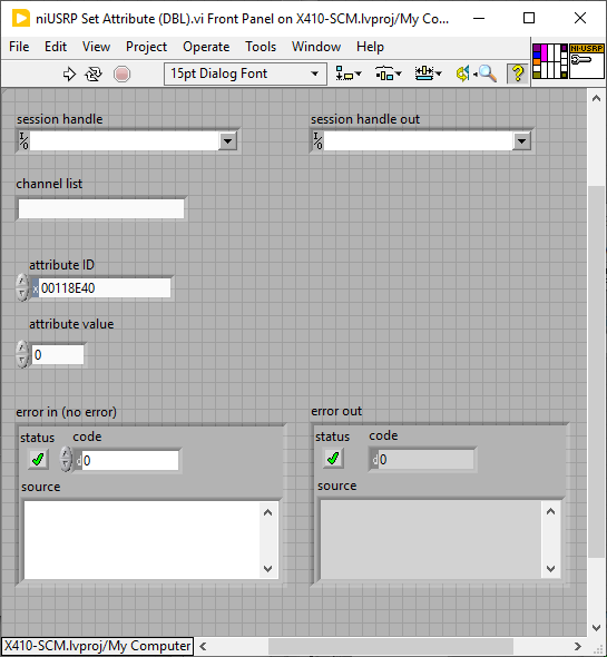
These are the DSP attributes that can be changed:
1. DSP Attribute: DCOffsetReal Type: double Attribute ID: 0x118E34
2. DSP Attribute: DCOffsetImaginary Type: double Attribute ID: 0x118E35
3. DSP Attribute: DigitalGainReal Type: double Attribute ID: 0x118E3D
4. DSP Attribute: DigitalGainImaginary Type: double Attribute ID: 0x118E3E
5. DSP Attribute: DigitalPreGainReal Type: double Attribute ID: 0x118E3F
6. DSP Attribute: DigitalPreGainImaginary Type: double Attribute ID: 0x118E40
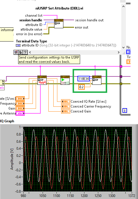
Here is an example of where this is used to add a DC offset using the DCOffsetReal attribute in the RX DSP path. You can see that the real component is now shifted up by 0.2V compared to the imaginary component.
Streaming Engine and optimization
With FPGA compiles there are tradeoffs between a number of features and speed versus resource usage. Thus, you will have a greater bitfile compilation success rate if you compile a 1spc bitfile v.s. a 4spc as well as using smaller FIFOs and disabling DSP features you do not need. The two flavors installed (4ch-1spc and 4ch-4spc) are just examples. If your solution only requires 1 channel at 4spc, it is more efficient to set up a project that compiles a 1ch-4spc bitfile instead of enabling 1 channel in a 4ch-4spc bitfile. Here are some parameters you can adjust.
FIFO Size
|
FIFO Type/Name
|
Size
|
|
Target to Host DMA FIFO (Rx Stream)
|
65535
|
|
Host to Target-FIFO (Tx Stream)
|
16479
|
When transferring acquired data through the Target to Host DMA FIFO, there are several limiting factors. There is the speed of the PCIe bus which will limit the number of samples you can fetch using finite acquisition at high rates since the IQ rate is greater than the PCIe speed. At an IQ rate of 491.52M, the speed of the PCIe bus will result in you retrieving a finite number of samples less than the size of the Rx Stream FIFO. At slower rates, the PCIe bus speed is not the limiting factor, and the host side buffer becomes the limiting factor resulting in more finite samples being transferred.
Continuous streaming to the host will be limited by the PCIe speed. The max PCIe speed is slower than the full 491.52M IQ rate thus you can’t keep up. Streaming data from the FPGA over Aurora would be an alternative.
Streaming Benchmarks
Below are some benchmarks on streaming performance. These benchmarks were done on the following equipment:
-
PXIe-8880 controller
-
PXIe-1095 chassis
|
i16 data
|
TX
|
RX
|
TX + RX
|
|
1 ch
|
491.00M
|
491.00M
|
165.00M
|
|
2 ch
|
263.00M
|
372.00M
|
83.00M
|
|
4 ch
|
136.00M
|
143.00M
|
41.00M
|
|
Complex Double data
|
TX
|
RX
|
TX + RX
|
|
1 ch
|
265.00M
|
404.00M
|
165.00M
|
|
4 ch
|
79.00M
|
81.00M
|
40.00M
|
DSP
In the shipping Reference Project, these DSP VIs are enabled.
|
ACQ_DIGITAL_OFFSET
|
Enabled
|
|
ACQ_DIGITAL_GAIN
|
Enabled
|
|
ACQ_EQUALIZATION
|
Disabled
|
|
ACQ_FREQUENCY_SHIFT
|
Enabled
|
|
ACQ_IQ_IMPAIRMENTS
|
Enabled
|
|
ACQ_DECIMATION
|
Fractional
|
|
GEN_DIGITAL_OFFSET
|
Enabled
|
|
GEN_DIGITAL_GAIN_PRE
|
Enabled
|
|
GEN_EQUALIZATION
|
Disabled
|
|
GEN_FREQUENCY_SHIFT
|
Enabled
|
|
GEN_IQ_IMPAIRMENTS
|
Enabled
|
|
GEN_INTERPOLATION
|
Fractional
|
|
GEN_DIGITAL_GAIN_POST
|
Enabled
|
Reduced resource usage can be obtained by disabling other DSP functions, especially when compiling a 4 spc bitfile.
Bit packing/FIFO optimization
The Reference FPGA project uses bitpacking to optimize transfers between the host and the target.
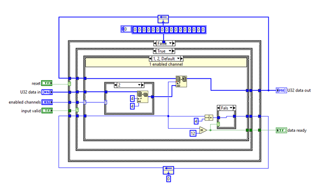
The Reference FPGA X410.vi (FPGA) can, as mentioned earlier, through Conditional Disable symbols be configured to only use 1 or 2 channels in a 4 channel configuration, or 1 channel in a 2 channel configuration. To optimize the Tx and Rx FIFO which is configured for 4 elements in a 1 spc configuration and 16 elements in a 4 spc configuration the stream engine will fill up all elements in the FIFO regardless of how many channels are enabled.
For the Tx stream controller, this FIFO logic is found in this sub VI:
.. \niUSRP\Reference FPGA\Stream Control\Protected\Tx Disable channel logic 2ch 4SPC.vi

The equivalent code for the Rx stream controller is found in this sub VI:
..\niUSRP\Reference FPGA\Stream Control\Protected\RX Disabled channel logic 2ch 4SPC.vi
General Notes
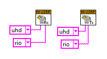
- If you are using UHD configuration and Rio streaming in niUSRP Open Rx Session with Custom Bitfile.vi or niUSRP Open Tx Session with Custom Bitfile.vi, then this optimization cannot be turned off.
- Be aware that support for the NI Ettus USRP X410 device was introduced in version 21.0 of the NI-USRP driver. You must install this version or a newer one to access the example explained here. Also, be aware this device is only supported in LabVIEW 2020 or newer.