PXIe-5785:
Analog Input:
To get the maximum sample rate of 6.4GS/s on the analog input in a single sample mode, the ADC interleaving factor has to be set to ‘2’ (the default is ‘1’) and only ‘AI0’ has to be enabled. The “Basic” host VI in the default NI PXIe-5785 LabVIEW example contains the relevant controls on the front panel that can be configured.
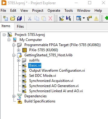
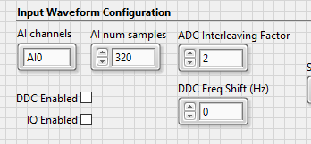
On the block diagram, the ADC interleaving factor is adjusted using the property node.

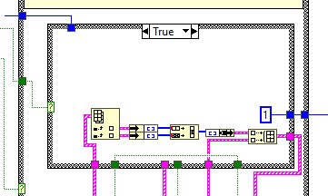
On the FPGA level, the data from the ADC (and CLIP) at 6.4GS/s is streamed to the FPGA through the same interface as of AI0 and AI1 (as deinterleaved streams) and later interleaved together before sending it to the host. The following is the relevant portion on the FPGA top-level VI that interleaves the data.
Analog Output:
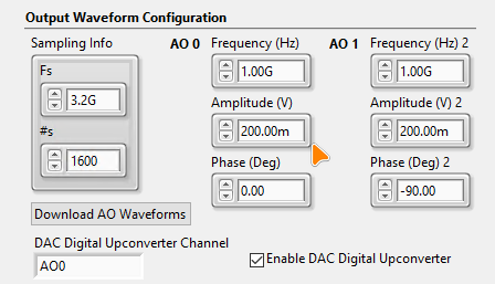
For the maximum rate of 3.2GS/s (complex) on the analog output of NI PXIe 5785, either choose “DAC and FPGA, One Channel” or “DAC-only, One Channel” in the “Output Waveform Configuration” section on the front panel:
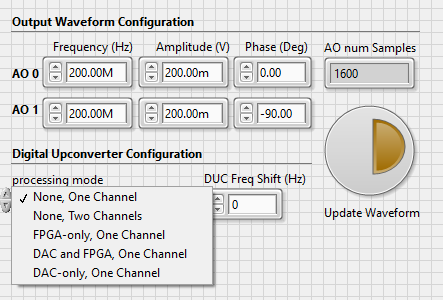
When choosing the “DAC and FPGA, One Channel” option, the host provides the AO complex (I and Q) data at 1.6GS/s. This data is further interpolated by the FPGA DSP algorithm to bring it at 3.2GS/s and later DAC digitally upconverts it by 1.6GHz to generate a complex output.
When choosing the “DAC-only, One Channel”, the host provides the AO complex (I and Q) data directly at 3.2GS/s to the FPGA, and later DAC digitally upconverts it by 1.6GHz to generate a complex output.
The “Output Waveform Configuration.vi” subVI in the getting started example for NI PXIe-5785 performs these configurations.
PXIe-5745:
Analog Output:
You can accomplish the same on the PXIe-5745 on the shipping example by toggling on the "Enable DAC Digital Upconverter" setting. Please take into account that the Enable DAC Digital Upconverter is not a tune-able setting.
When you enable the DAC DUC, in the default example, is that AO0 and AO1 are treated as I and Q and the complex data center frequency is now fixed at 1.6 GHz with an effective real bandwidth of 3.2 GHz:
