Introduction to SPI
The SPI bus is a 4-wire, full-duplex serial interface. Three of the wires, SCK, MOSI (master output, slave input), and MISO (master input, slave output), are shared along with a fourth wire, known as the chip select (CS), which is a direct connection between the master and a single slave device. When using multiple devices, the chip select determines which device is currently active and initiates communication with that device. The master-slave relationship is key to understanding how SPI works. The SPI master device provides the clock signal and determines the chip select line state. The slave device(s) receive the clock and chip select signals. The USB-8451 is always the master device because it provides the clock signal (SCK) and the cable select lines.
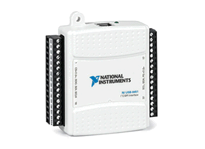
Figure 1. NI USB-8451 I2C and SPI Interface
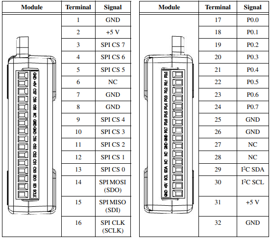
Figure 2. NI USB-8451 pinout
Communication across SPI uses a system known as data exchange. Whenever a bit is written to an SPI device across the MOSI line, the SPI device concurrently returns a bit on the MISO line. Because data is transferred in both directions, it is up to the receiving device to know whether the received bit is meaningful or not. For example, to receive data from an EEPROM, the master must configure the EEPROM to send n bytes of data and then must send n bytes to be exchanged for valid data. Depending on the device, these bytes can usually be any value, i.e., dummy data, and writing them serves only to clock the data out of the receiving device. In other cases, an instruction may be written to the MOSI line that directs the SPI slave device to output specific data. For example, many ADCs require the user to write an 8-bit instruction that specifies a register to read. After that instruction is written, a delay is required, followed by dummy data that is written to the slave device (MOSI) to clock out the specified data. In the NI-845x API, you can implement such communication schemes by means of the SPI Advanced palette, with which you can create custom SPI scripts for implementing variations of SPI and other serial protocols.
Installation and Configuration of the USB-8451
The USB-8451 uses a LabVIEW API consisting of references, property nodes, and functions. You must install this driver from the included driver CD or by visiting the NI website: Drivers and Updates: NI-845x Driver Software.
- After installing the driver software, install the USB-8451 by plugging it into an open USB port.
- After completing the Microsoft Windows installation procedure, open Measurement & Automation Explorer (MAX) and expand the Devices and Interfaces folder. Because the USB-8451 is installed as a RAW USB device, it appears under USB devices as shown in figure 2.
- To configure a VISA alias for use in LabVIEW, expand the USB Devices folder, left click on the USB-8451 and enter a new VISA alias in the text box entitled VISA Alias on My System.
- After a new name has been entered, click Save and then exit MAX.
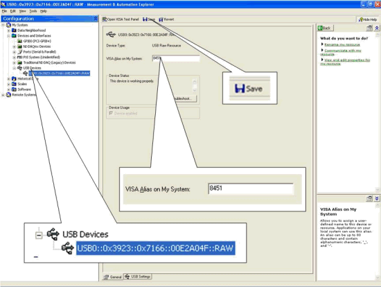
Figure 3. In MAX, the USB-8451 appears under My System >> Devices and Interfaces >> USB Devices. To change the VISA alias, left click on the USB-8451 under USB Devices, enter a new “VISA Alias on My System,” and click Save.
Now that the VISA alias has been configured in MAX, you can now use the alias in the NI-845x device reference in LabVIEW.
Gathering Information
For this example, we will be evaluating the Texas Instruments ADS1224, 24-bit, 240 S/s, 4-channel, analog-to-digital converter. This data converter is used in applications where high precision and relatively low sampling speeds are required. Examples include hand-held instrumentation, scales, and portable instrumentation.
Instead of choosing the bare Texas Instruments ADS1224 ADC and integrating the required external parts (capacitors, DC-DC converter, etc), Texas Instruments provides an evaluation module, the TI ADS1224EVM, complete with all the necessary parts.
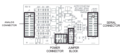
Figure 4. Texas Instruments ADS1224EVM Board Layout.
The ADS1224EVM contains three header blocks for connecting the analog input signal, power supply, and serial output. In addition, a series of switches and jumpers are available to configure settings such as the ADC voltage reference, the input select, and the digital power select. Before making any connections to the evaluation module or writing any code, we must examine the data sheet for the ADS1224 and the ADS1224EVM to determine the proper jumper and switch settings to place the ADS1224EVM in a mode compatible with the USB-8451.
Upon close examination of the ADS1224 user manual, pages 13-16, it becomes clear that the serial output is not pure SPI, but a slightly different serial protocol implemented as 2-wire serial. The USB-8451 offers advanced functionality that allows for flexibility and ultimately, the ability to support different flavors of serial protocols, not just pure SPI or I2C. As we continue to examine the ADS1224 data sheet, we see that the serial output connector contains two terminals relevant to the serial data transfer: SCLK (input) and DOUT/DRDY (output). The SCLK line, also known as the serial clock, is an input to the ADC that clocks data bits out of the ADC onto the DOUT/DRDY line. Each SCLK clock cycle input into the ADC produces one output bit, representing the conversion produced from the ADC. Because the ADS1224 is a 24-bit ADC, we need to clock out 24-bits to obtain each ADC conversion result.
The DOUT/DRDY line is a multifunction line serving to transfer the serial data and to alert the device that a new conversion result is ready to be transferred to the USB-8451. When the normally high DOUT/DRDY line transitions to a low state, a conversion is ready to be output from the ADS1224. After this low signal is received, 24-bits of data are ready to be clocked out.
There are four other inputs to the ADS1224 that define its behavior. The first two are digital input lines MUX0 and MUX1. These inputs define the analog input channel which will be read. In our case, setting MUX0 and MUX1 low specifies that the ADS1224 will read channel 0. Another input, TEMPSEN, when enabled, bypasses the external analog inputs and outputs a voltage from an on-board temperature sensor to the ADC. The last input, BUFEN, enables a built-in buffer circuit. The buffer circuit would be useful in applications where a high impedance signal source is used, but in this example, a low impedance source is used so BUFEN is disabled.
Making the Connections
Now that we understand the basics of how the ADS1224 works, we are ready to connect it to the USB-8451. To begin, we examine the analog input connector; the input to the ADC. For simplicity we configure channel 0 of the ADC for a differential measurement by connecting AN0+ and AN0- to our signal source. The power connector, J3, requires four connections: +5 V analog and digital supply, and analog and digital grounds. Because the USB-8451 contains a +5 V supply, we can power the evaluation module directly from the USB-8451. Before making the connection to the USB-8451, make sure +5VD (pin 9) is shorted to DVDD (pin 10) on the ADS1224EVM jumper block. This configures the ADS1224 to use a +5 V input. Alternatively, we could use a 1.8 or 3.3 V digital supply. Next, we connect both +5 V analog and digital supplies to the USB-8451 +5 V terminal and the analog and digital grounds to the 8451 ground connector. Now that we have connected the analog input signal and the power to the ADS1224EVM, we need to connect the serial output to the USB-8451.
The following settings and connections were used for the evaluation of the Texas Instruments 1224EVM:
Analog Connector – J1
- Differential input zero (AN0+/AN0-) are connected to an analog output signal source (M-series DAQ card)
Power Connector – J3
- Analog and digital grounds (internally tied to ADS1224EVM ground) are connected to the USB-8451 ground input
- Positive analog supply (+5V) and positive digital supply (+5V) are connected to the +5V output of the USB-8451
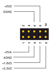
Figure 5. Header block for the Texas Instruments ADS1224EVM power supply. In this demonstration, the analog and digital grounds are tied to the USB-8451 ground input. The +5VD and +5VA were also connected together and connecting to the +5 V terminal of the USB-8451.
Header Connector
The header connector is used to configure the digital power supply for the ADC. In this case, we use the +5 V range by shorting pins 9 and 10 as shown below.
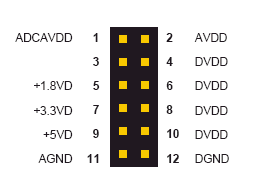
Figure 6. Jumper block for the Texas Instruments ADS1224EVM power supply. In this demonstration, Pins 9 and 10 are shorted to configure +5 V digital operation.
Serial Output Connector – J2
- SCLK (pin 3) is connected to USB-8451 SCLK output
- DOUT/DRDY are connected to USB-8451 MISO line
- MUX0, MUX1, BUFEN, and TEMPSEN are connected to the USB-8451 digital lines P0.0, P0.1, P0.2, and P0.3, respectively
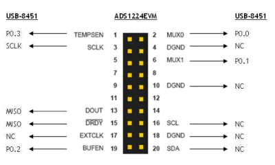
Figure 7. Header block for the Texas Instruments ADS1224EVM serial output. The arrows indicate the connections to the USB-8451 used in this demonstration.
Slide Switches
The slide switches on the ADS1224EVM configure what kind of signal is input to the ADC, whether we want to measure an onboard reference to test the accuracy of the ADC, or we want to configure the ADS1224 to perform a single-ended or differential measurement. The following switch settings were used in this evaluation.
| Switch Name | Position | Description |
S1
S2
S3
S4
S5
S6
S7 | EXT
EXT
EXT
EXT
2.5V
0V
OB | Ch 1 Input Switch
Ch 1 Input Switch
Ch 2 Input Switch
Ch 2 Input Switch
Voltage Reference Input Switch
Voltage Reference Input Switch
System clock source |
Table 1. Slide Switch Positions Used for the Texas Instruments ADS1224EVM
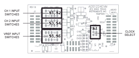
Figure 8. Slide Switches (S1-S7) on the Texas Instruments ADS1224EVM
Programming
The LabVIEW API provided for the USB-8451 provides two different APIs for programming I2C and SPI devices. The first method, known as the Basic API, involves using a minimum number of LabVIEW functions and is best suited for simple communication schemes that comply with the timing characteristics of the USB-8451. Figure 7, shown below, is an example of the LabVIEW API for basic SPI communication. The program can be broken into three distinct pieces. The first piece configures the 845x device by specifying the desired behavior of the digital lines. The second piece configures the SPI specific features such as the SCLK rate, the clock phase, the clock polarity, and the chip select line to use. This simple methodology will work for many devices, but the TI ADS1224 requires more advanced control over the specific timing of its serial communications. Specifically, the simple method of communication performs serial operations at a speed that is too fast for the ADS1224 to keep up. This results in corrupted data and inconsistent results. To solve this problem, we can use the Advanced API for the USB-8451that provide scripting functionality to effectively create custom transactions of the serial operations you wish to perform.
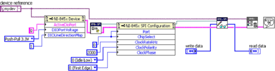
Figure 9. Simple SPI Example Using the LabVIEW Basic SPI VIs
When designing our program, we can break it into three pieces. The first piece is configuration. Here we configure the digital lines used to determine which analog input channel we are going to read, whether or not we are enabling the on-board buffer circuit, and whether we are going to read the on-board temperature sensor. In addition, we configure the properties of the serial clock such as the clock rate, polarity, and phase.
The second piece of the program is the script that will define how the serial protocol will function. For our program, we will set digital lines, wait for a period of time, and then clock out 24-bits of data (one conversion result). Finally, we execute the script we created on the USB-8451, transfer the data obtained, and perform the appropriate conversion on the data. In the case of the ADS1224, the data transferred is in the form of binary twos-complement. A custom VI was created, twos complement to voltage.vi, that converts the output data from the ADS1224 to voltage.
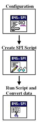
Figure 10. Programming Architecture for Example Program
The example program, attached below, is an implementation of the concepts and ideas discussed in the previous sections. The VI will communicate through the USB-8451 to the TI ADS1224 each time the “Press to take a Reading” button is pushed. Each reading will then be stored in a waveform chart.
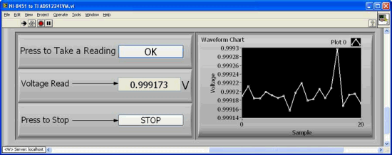
Figure 11. Screenshot of Example VI Measuring a 1 VDC Source
To view and download this example program, visit the Developer Zone Example: Using a NI USB-8451 I2C/SPI Device to Evaluate a Texas Instruments Analog-to-Digital Converter - Example Program.
Conclusions
The NI USB-8451 I2C and SPI device provides an excellent platform for evaluating electronic components such as analog-to-digital converters. Using the API included, you can integrate SPI, I2C, as well as other flavors of serial protocols via the built-in scripting functionality.
For more further information and ordering details for the NI USB-8451, please visit the Web page for the USB-8451.