Verilog Module
For the purpose of this tutorial, a simple Verilog module has been provided as a starting point. The file can be found in the attached files at the following location:
..\verilog_integration_tut\Adder.v.
Adder.v instantiates a clock driven, 8-bit adder with an asynchronous reset and clock enable. The following table shows the port definition for the component.
|
Port
|
Direction
|
Description
|
|
clk
|
in
|
Input clock that drives component
|
|
clkEn
|
in
|
Enable signal for clock-gating
|
|
aReset
|
in
|
Asynchronous reset
|
|
dataInA (7:0)
|
in
|
8-bit input data port A
|
|
dataInB (7:0)
|
in
|
8-bit input data port B
|
|
dataOut (7:0)
|
out
|
8-bit output data port
|
Integration Options
To integrate external or third-party IP into LabVIEW FPGA you can use Component-Level IP (CLIP) or the IP Integration Node (IPIN). While both allow the integration of code external to LabVIEW, these options have different use cases and limitations. NI recommends that you refer to the LabVIEW Help for the different design requirements before integrating any external IP.
One difference that is relevant to this tutorial is that the top-level synthesis file for CLIP must be a VHDL file while IPIN can use netlists as the top-level synthesis file. This means the generating a VHDL wrapper is required for CLIP but optional for IPIN. However, IPIN might require a VHDL wrapper in specific scenarios. For example, when a top-level port type of the Verilog module is not supported in LabVIEW.
Setting Up an ISE Project
To prepare a Verilog module for integration into LabVIEW FPGA, you must first create a project and configure it properly in the Xilinx ISE Design Suite.
-
Open Xilinx ISE Design Suite from Start » All Programs » Xilinx ISE.
-
Click File » New Project and configure the Create New Project page as shown below.
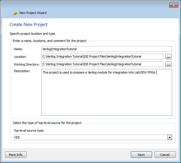
-
Click Next.
-
In the Project Settings page, configure the Family, Device, Package, and Speed settings as needed for your FPGA target. You can find the details for each target in the General section of the FPGA Target Properties window in LabVIEW. In this tutorial we will be preparing IP for use on a PXIe-7965R (FlexRIO).
- Select VHDL as the Preferred Language to ensure that files are always generated in VHDL.
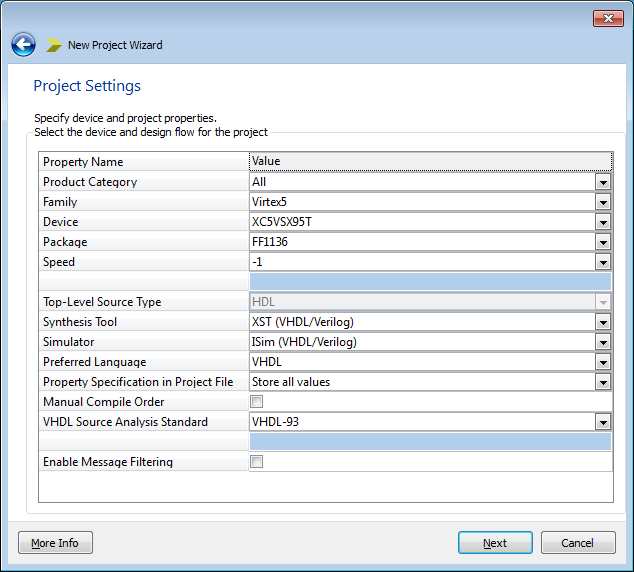
- Click Next until you reach the Project Summary page and then click Finish.
Adding a Top Level Source
- In the Design Implementation view, right-click the FPGA target and select Add Source.
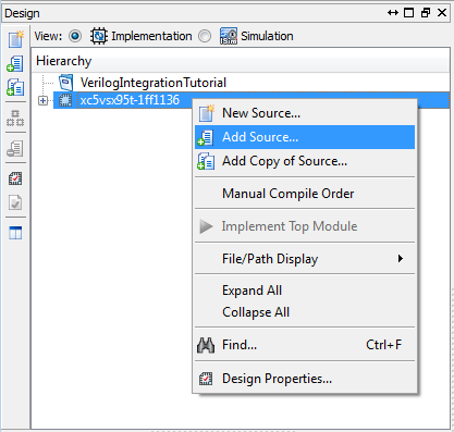
- Browse to the Adder.v Verilog module in the working directory and click Open.

-
Click OK to add the Verilog module to the project.
Synthesizing the Design
After the Verilog module is added to the project, it must be synthesized into a supported netlist format that can be used by a VHDL module. This tutorial uses the NGC format.
-
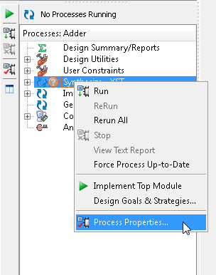
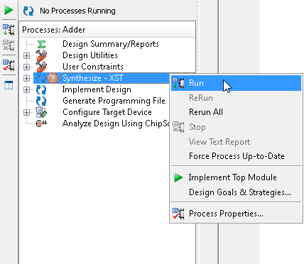
In the Design Implementation view, click Adder (Adder.v).
-
In the Processes view, right-click Sythesize-XST and select Process Properties..
-
Select the Xilinx Specific Options category in the Process Properties window.
-
Set the Add I/O Buffers property to FALSE. There will be no direct FPGA pin connections when we use this component within a LabVIEW FPGA design, making these buffers unnecessary.
- Set the value of the Pack I/O Registers Into IOBs property to No.
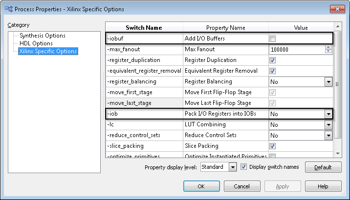
-
Click Apply to save changes and click OK to exit the Process Properties window.
- In the Processes view, right-click Synthesize-XST and click Run.
- During Synthesis, a Xilinx NGC netlist file named Adder.ngc is created. This netlist is synthesized code which defines the component that will be wrapped. In the working directory for the ISE project, find the Adder.ngc file and note its location.
Creating the VHDL Simulation Model
Creating a VHDL simulation model allows you to accurately simulate the behavior of a Verilog module from a VHDL context.
Note: This step is required only if you plan to simulate Component-Level IP in a third-party simulator such as Xilinx ISIM. In the case of the IP Integration Node, the simulation behavior can be set to a Post-synthesis model for simulation purposes within the LabVIEW environment. As Component-Level IP cannot be directly simulated within LabVIEW FPGA, excluding the netlist from the simulation model will allow full functionality for most use cases. For more information on debugging LabVIEW FPGA code through simulation, see Testing and Debugging LabVIEW FPGA Code.
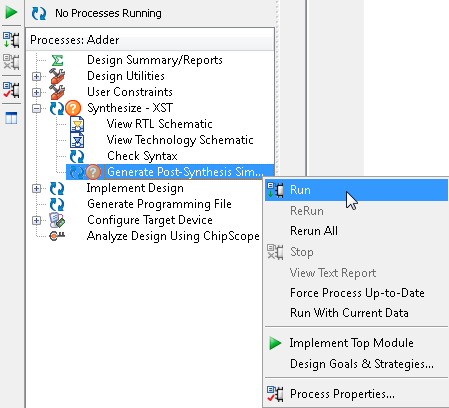
- Expand Synthesize-XST, right-click Generate Post-Synthesis Simulation Model and select Run.
-
A post-synthesis VHDL simulation model is created. In the working directory, find Adder_synthesis.vhd and note its location.
Creating a VHDL Wrapper
To integrate an NGC netlist into LabVIEW FPGA, you must create a VHDL wrapper file that instantiates the component. Creating this file generally is not difficult, but it may require some knowledge of the VHDL language.
-
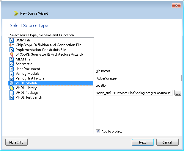
In the Design Implementation view, right-click the FPGA target and select New Source.
- Create a new VHDL module by configuring the window as shown below.
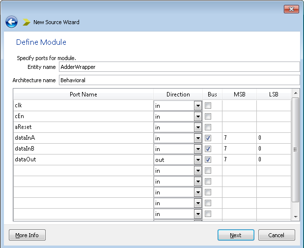
- Click Next to proceed to the Define Module page. Configure the page as shown below. Ensure that the ports defined for the VHDL wrapper module match the ports defined in the original Verilog module. Wrapper modules require a set of ports that correspond to the original IP.
- Click Next until you reach the Summary page and then click Finish.
-
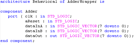
Instantiate the Adder component in the architecture declarations of the VHDL module as shown below.
-
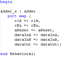
Map the ports from the Adder component to the top-level ports of the AdderWrapper.
-
Click File » Save.
Integrating the IP into LabVIEW
Once you have synthesized the Verilog module into a netlist and created a VHDL wrapper, the standard IP integration procedure for either CLIP or IP Integration Node applies.
-
Gather the required HDL and synthesis files. You will need the VHDL wrapper and all netlists as well as their simulation models. For this design you will need the following files:
-
AdderWrapper.vhd - The VHDL wrapper created in this tutorial for the Verilog Module. This will be the top-level module.
-
Adder.ngc - The synthesized netlist for the Verilog Module.
-
Adder_synthesis.vhd - The simulation model for the Verilog Module netlist. To use this when importing the IP into LabVIEW, set the simulation behavior of Adder.ngc to User-Defined and select this file.
-
Follow the steps in the Importing External IP Into LabVIEW FPGA Tutorial to integrate the IP into LabVIEW FPGA. Use the files listed above when choosing synthesis files.