Required Software and Files
To complete this tutorial, you must have the following software installed:
- LabVIEW Development Environment
- LabVIEW FPGA Module
- LabVIEW FPGA Module Xilinx Compilation Tool for Vivado
You must download and extract the attached zip folder which contains all the source files that will be used throughout the tutorial and the IP integrated through both CLIP and IPIN.
Note: This document was created using LabVIEW 2018 and Vivado 2017.2. The steps and UI text may differ in other LabVIEW or Vivado versions.
Verilog Module
For the purpose of this tutorial, a simple Verilog module has been provided as a starting point. The file can be found in the attached folder at the following location:
..\vivado_verilog_tutorial\Source Files\Adder.v
Adder.v instantiates a clock driven, 8-bit adder with an asynchronous reset and clock enable. The port definition for this component is shown in the table below.
| Port | Direction | Description |
|---|
| clk | in | Input clock that drives the component |
| clkEn | in | Enable signal for clock-gating |
| aReset | in | Asynchronous reset |
| dataInA (7:0) | in | 8-bit input data port A |
| dataInB (7:0) | in | 8-bit input data port B |
| dataOut (7:0) | out | 8-bit output data port |
Integration Options
To integrate external or third-party IP into LabVIEW FPGA you can use Component-Level IP (CLIP) or the IP Integration Node (IPIN). While both allow the integration of code external to LabVIEW, these options have different use cases and limitations. NI recommends that you refer to the LabVIEW Help for the different design requirements before integrating any external IP.
One difference that is relevant to this tutorial is that the top-level synthesis file for CLIP must be a VHDL file while IPIN can use netlists as the top-level synthesis file. This means the generating a VHDL wrapper is required for CLIP but optional for IPIN. However, IPIN might require a VHDL wrapper in specific scenarios. For example, when a top-level port type of the Verilog module is not supported in LabVIEW.
Setting Up a Vivado Project
To prepare a Verilog module for integration into LabVIEW FPGA, you must first create a project and configure it properly in the Xilinx Vivado Design Suite.
Note: The LabVIEW FPGA Module Xilinx Compilation Tool for Vivado installs the Vivado Design Suite, which uses the same compiler version and configuration as the LabVIEW FPGA Module. NI recommends that you use this version of Vivado Design Suite for preparing any third-party or external IP for integration into LabVIEW FPGA when using Vivado FPGA targets.
- Launch the Xilinx Vivado Design Suite installation that installs with the LabVIEW FPGA Module Xilinx Compile Tool for Vivado by running the following batch file:
C:\NIFPGA\programs\<Vivado>\bin\vivado.bat - Click File » New Project... to start the New Project wizard, then click Next.
-
Configure the Project Name page as shown below.
- Click Next to advance to the Project Type page, ensure that RTL Project is selected, then click Next again.
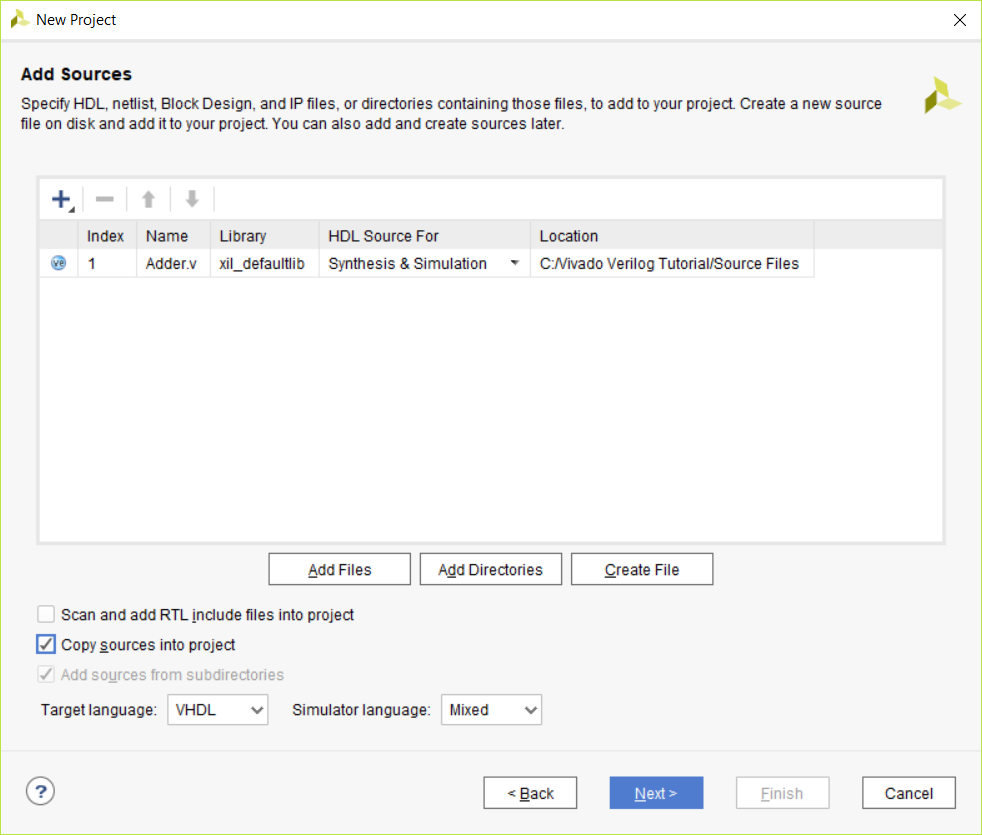
- In the Add Sources page, add the Adder.v Verilog module and select VHDL in the Target Language drop-down.
- Click Next, and then click Next again to proceed to the Default Part page.
-
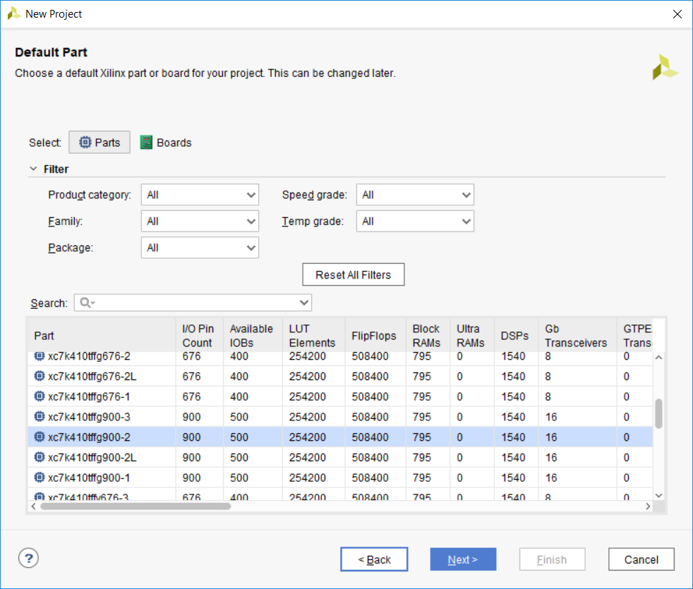
Select the part that matches the FPGA device you will be using in your LabVIEW FPGA project. You can find the details for each target in the General section of the FPGA Target Properties window in LabVIEW. In this tutorial we will be preparing IP for use on a PXIe-7975R (FlexRIO).
- Click Next, and then Finish to complete the setup process.
Synthesizing the Design
Once the project is configured and all source files have been added, the Verilog module must be synthesized into a netlist following the Hierarchical Design
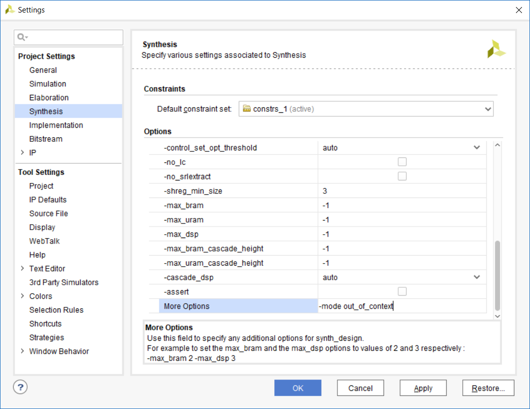
flow. This means that the synthesis must be performed in out-of-context (OOC) mode to allow the Verilog module to be used from a VHDL context. This tutorial uses the .dcp netlist file format.
- Under the Project Manager, click Settings.
- Under Project Settings, select Synthesis.
- In the Options section, enter -mode out_of_context in More Options.
- Click Apply and then OK.
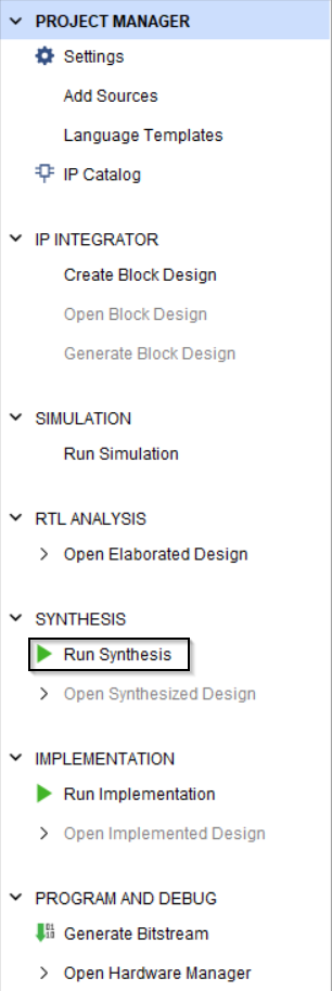
- Under the Project Manager, click Run Synthesis.
- In the Launch Runs window, click OK to begin the synthesis.
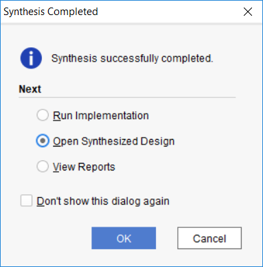
- When the synthesis is complete, in the Synthesis Completed window select Open Synthesized Design and click OK.
-
As a result of synthesis, a .dcp netlist will have been created. The netlist is synthesized code which defines the component to be wrapped. In the working directory for the Xilinx Vivado Design Suite project, the .dcp file should be located at the following location. Make note of this file location.
..\VerilogIntegrationTutorial.runs\synth_1\Adder.dcp
Note: .dcp files are not forward version compatible. NI recommends that you generate these files using the installation of the Vivado Design Suite provided for the version of LabVIEW you are working in.
Creating a VHDL Wrapper
To integrate a .dcp netlist into LabVIEW FPGA, you must create a VHDL wrapper file that instantiates the component. Creating this file is generally not difficult, but may require some knowledge of the VHDL language.
- In the Sources view, right-click Design Sources and select Add Sources...
-
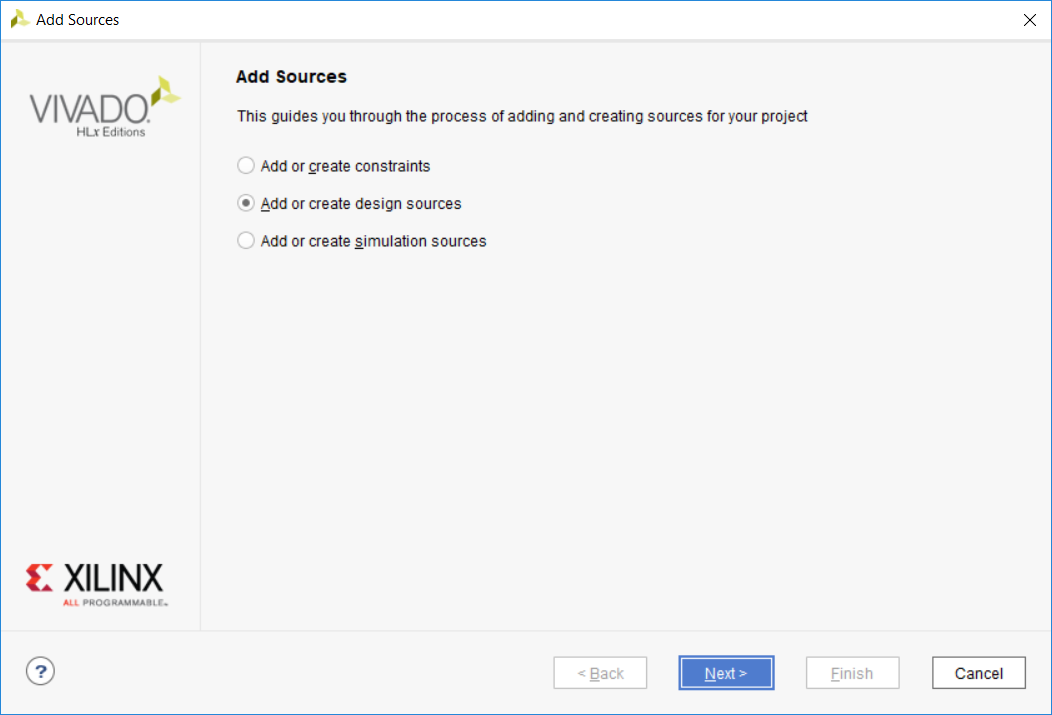
In the Add Sources window, select Add or create design sources and then click Next.
- Click Create File.
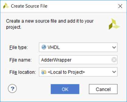
- Configure the Create Source File window as shown below and click OK.
- Click Finish.
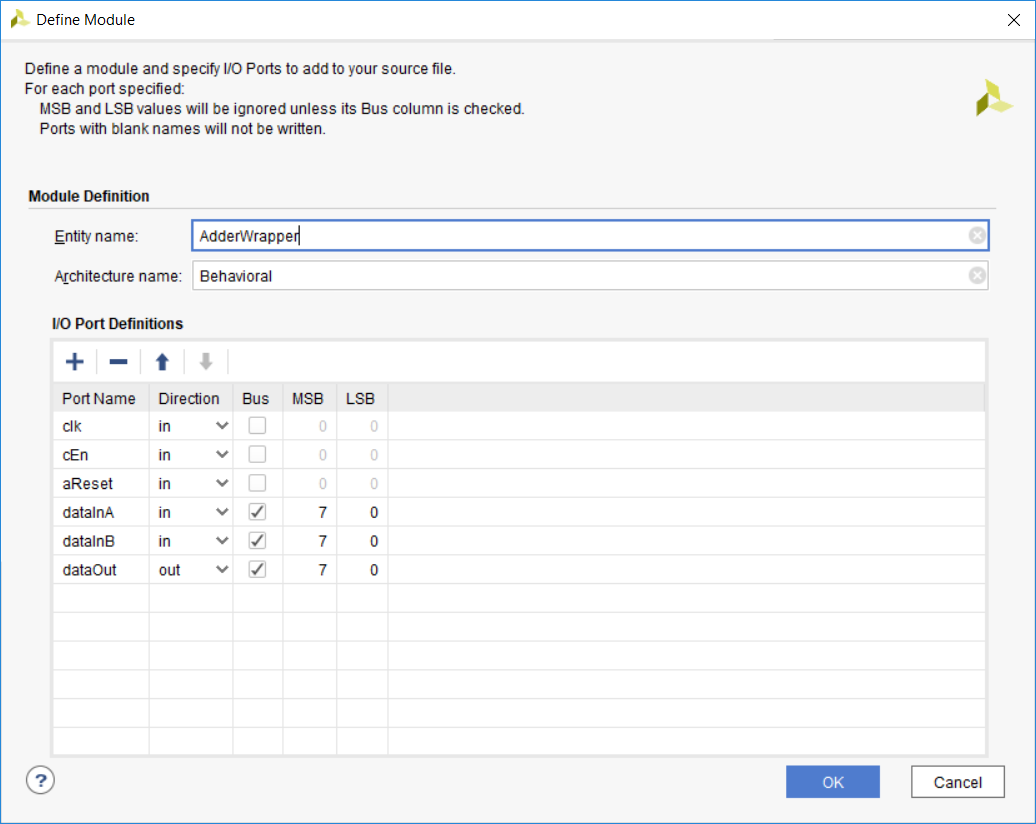
- Configure the Define Module window as shown below. Ensure that the ports defined for the VHDL wrapper module match the ports defined in the original Verilog module. Wrapper modules require a set of ports that correspond to the original IP.
- Click OK.
- Double-click the new source file under Design Sources in the project to open the file in the editor.
- Instantiate the Adder component in the architecture declarations of the VHDL module as shown below.

- Map the ports from the Adder component to the corresponding top-level ports of the AdderWrapper entity.
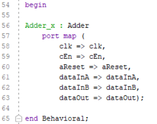
- Save the modified wrapper file.
Integrating the IP into LabVIEW
Once you have synthesized the Verilog module into a netlist and created a VHDL wrapper, the standard IP integration procedure for either CLIP or IP Integration Node applies.
- Gather the required HDL and synthesis files. You will need the VHDL wrapper and all netlists. For this design you will need the following files:
- AdderWrapper.vhd - The VHDL wrapper created in this tutorial for the Verilog Module. This will be the top-level module.
- Adder.dcp - The synthesized netlist for the Verilog Module.
- Follow the steps in the Importing External IP Into LabVIEW FPGA Tutorial to integrate the IP into LabVIEW FPGA. Use the files listed above when choosing synthesis files.
Advanced Integration Using the Tcl Console
While the above tutorial walks through the process many users may find most intuitive, it may be quicker to generate the necessary files using the Tcl Console from within the Vivado Design Suite. The Tcl Console allows you to run many of the underlying commands used by the Vivado GUI directly and exposes other advanced options. In some situations, using these commands may be more straightforward or quicker than using the GUI. For the purpose of this tutorial, the focus will be on implementing the same options as above using the console. For more information on the functions used below, refer to the official Xilinx documentation.
Note: The exact behavior and format of these commands may differ between versions of the Xilinx Vivado Design Suite. NI recommends that you read the Xilinx documentation for these commands before proceeding.
Synthesis
To perform synthesis and generation of the netlist, first create a Vivado project and add the Adder.v Verilog Module to the project. Once the module is addded to the project, take note of the name of the entity in the Sources view. In the example case of the Adder.v Verilog module, the name of the entity within the project is Adder. To run the synthesis process, you can use the the synth_design command from the Tcl Console. For the Adder module used in this tutorial, the command might look like this:
synth_design -top Adder -part xc7k410tffg900-2 -mode out_of_context
Once synthesis is complete, generate the netlist file using the write_checkpoint command.
write_checkpoint -force -noxdef "C:/Vivado Verilog Tutorial/Adder.dcp"
This command generates the .dcp netlist file at the location specified. Alternatively, you can use the write_edif command to generate an EDIF netlist. Refer to the official Xilinx documentation for information on using the write_edif command in the Tcl Console.
Writing a VHDL Wrapper
To write a VHDL Wrapper, the same process detailed in the Creating a VHDL Wrapper section of this document can be used. Alternatively, you can use the write_vhdl command to generate a stub VHDL file which you can use to integrate the Verilog module. This would be equivalent to steps 1 through 7 in the Creating a VHDL Wrapper section above and you would still need to go through the remaining steps. Additionally, you must add the new .vhd file to the project or edit it manually in another editor. To generate such a stub file, execute the following command.
write_vhdl -mode port "C:/Vivado Verilog Tutorial/AdderWrapper.vhd"
Creating a Functional Simulation Model
Note: This step is required only if you plan to simulate Component-Level IP in a third-party simulator such as Xilinx ISIM. In the case of the IP Integration Node, the simulation behavior can be set to a Post-synthesis model for simulation purposes within the LabVIEW environment. As Component-Level IP cannot be directly simulated within LabVIEW FPGA, excluding the netlist from the simulation model will allow full functionality for most use cases. For more information on debugging LabVIEW FPGA code through simulation, see Testing and Debugging LabVIEW FPGA Code .
If you want to simulate your module within LabVIEW FPGA, NI recommends that you generate a VHDL simulation model for the netlist using the write_vhdl command with different flags than used previously. You can then use the simulation model as the user-defined simulation behavior in LabVIEW FPGA. To generate a functional simulation model for the Adder module, execute the following command.
write_vhdl -mode funcsim "C:/Vivado Verilog Tutorial/Adder_funcsim.vhd"