FPGAs for Wireless Engineers Series: Immediately Connect Your FPGA Algorithms to I/O

Updated Aug 20, 2021

Environment

Hardware

  • USRP Software Defined Radio Device

Software

  • LabVIEW Communications System Design Suite
  • LabVIEW FPGA Module

Wireless engineers often want to use over-the-air signals to go from concept to prototype. Software defined radios (SDRs) such as the USRP (Universal Software Radio Peripheral) device provide a flexible solution to meet that need. With today’s applications demanding higher bandwidths and lower latencies, more of this signal processing needs to be implemented on the FPGAs of SDRs. However, wireless engineers programming FPGAs often face the following challenges:

1. Difficulties interfacing between FPGAs and inputs/outputs such as RF signals or the host CPU
2. Unfamiliar programming paradigms for algorithm implementation, and
3. Long compile times

In this series on FPGA Prototyping for Wireless Engineers, learn how the LabVIEW Communications System Design Suite (LabVIEW Communications) and NI SDR hardware can help you overcome each of these key challenges and quickly create real-time, over-the-air testbeds without FPGA knowledge.
 

FPGA designs typically require multiple components of VHDL code for interfaces such as analog-to-digital converters (ADCs)/digital-to-analog converters (DACs), PCI Express buses, memory, and clocks (Figure 1a). Each of these is typically developed from scratch, reused from existing designs, or acquired IP from Xilinx or other IP vendors. This means significant integration work—often more work than the actual algorithm implementation itself—must be completed to get all these pieces to connect.


Though these hardware interfaces are challenging to implement, customizing them rarely offers any value. With the ADC interface, for example, closing static timing and working out synchronization may be difficult, but the function of converting analog inputs to digital samples is relatively the same from project to project. To remove this bottleneck, LabVIEW Communications provides the interfaces to all the hardware on the SDR printed circuit board (PCB) out of the box. For example, ADC data is presented to the FPGA diagram as samples that have already been properly sampled and converted to the right data type, and you can simply drop a Read I/O node on your diagram to access them. Similarly, to stream data from the FPGA to the CPU, you just need to use a Write FIFO node and not worry about the actual streaming implementation itself.


The first installment to this "FPGA Prototyping for Wireless Engineers" series shows you how to leverage LabVIEW Communications to immediately move data on and off the FPGA so you can stay focused on implementing your algorithms.

Figure 1. (a) In a typical custom FPGA design with I/O, design teams often spend more time integrating I/O interfaces than implementing their algorithms or IP. (b) In LabVIEW Communications, those interfaces are already implemented so design teams can focus on implementing their signal processing instead of system integration.

1. Drop I/O Nodes

To interface FPGA algorithms with the ADCs and DACs that connect to the RF front ends, a host CPU, or resources such as memory, simply drop a Read or Write node for that resource. See Figure 2 for some examples of these nodes.

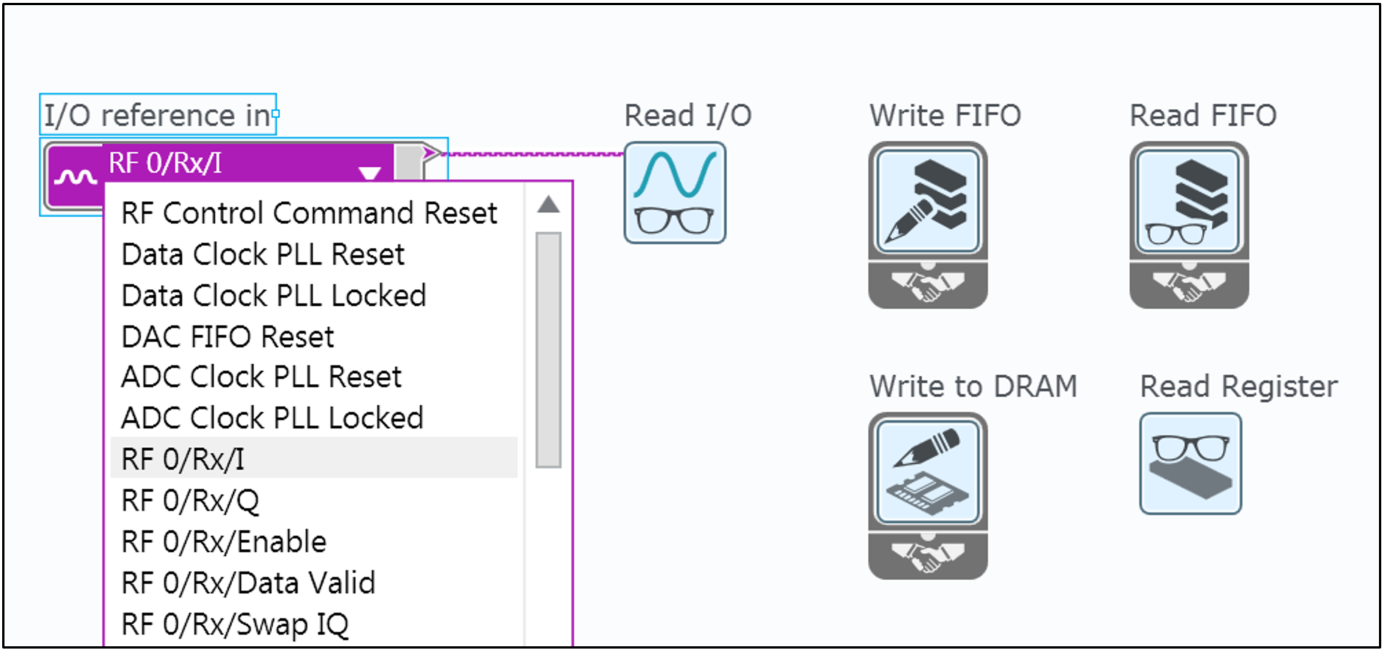
Figure 2. Use blocks like these to communicate with real-world I/O, FIFOs moving data to and from the host CPU, the DRAM on the USRP RIO device, or registers.
 

2. Configure I/O Nodes

You can configure FPGA I/O resources using a resource file, as shown in Figure 3. Configure properties like resource alias, data type, direction (FPGA to host, host to FPGA, FPGA to FPGA, local), or buffer depth.
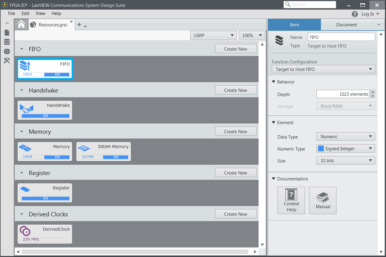
Figure 3. Use a resource file to create and configure FIFOs, memory, clocks, and other resources.
 

3. Connect Algorithms to I/O Nodes

Once you have created and configured your desired resources, you can connect them to the algorithms you implement on the FPGA. For example, the block diagram in Figure 4 was implemented on the FPGA in LabVIEW Communications (see Figure 5). In the design, data from the receive port of the USRP RIO device is streamed into “My Algorithm” on the FPGA, which could be any block like synchronization, demodulation, or a filter. The output is then streamed to memory and an FPGA-to-CPU FIFO.

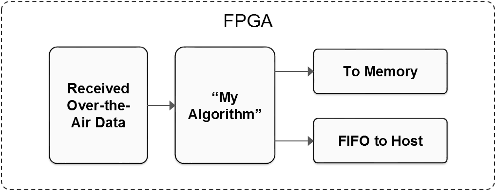
Figure 4. This block diagram of the example design shows how data is received from the RF front end, processed by a user-created block called “My Algorithm,” and streamed to memory and the host CPU. My Algorithm could be any algorithm such as demodulation, filters, or fast Fourier transforms.


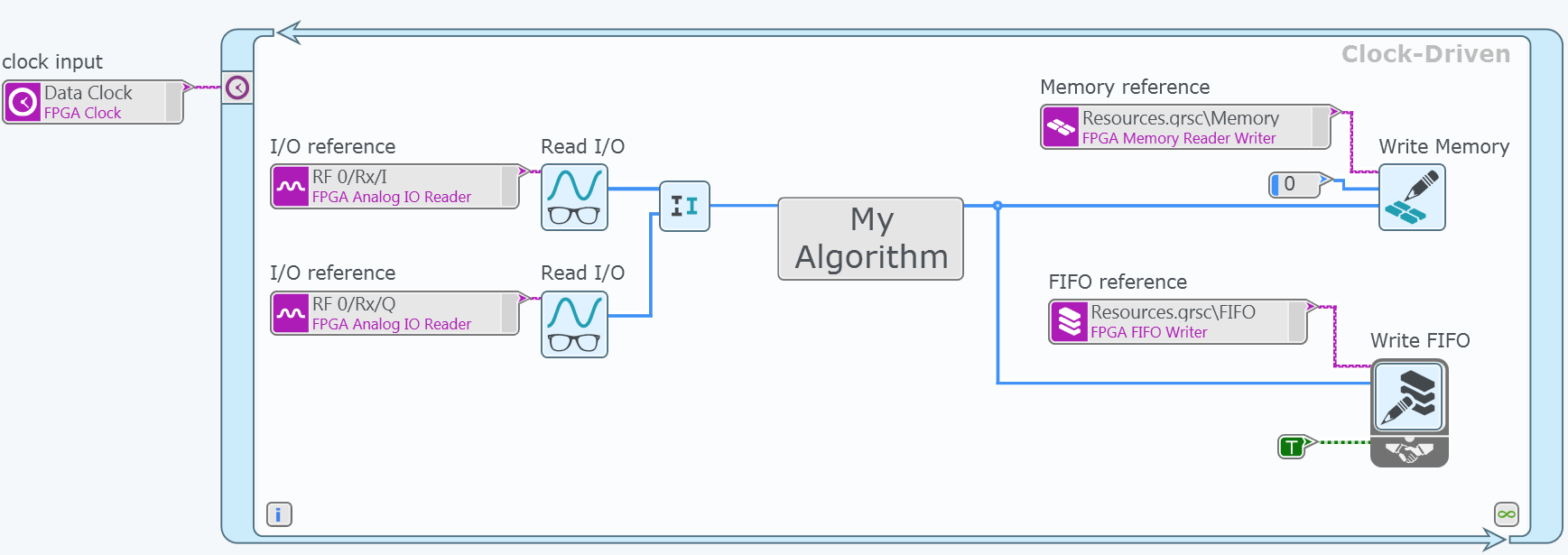
Figure 5. In this implementation of the theoretical block diagram in FPGA code in LabVIEW Communications, raw I and Q data is read from the RF front end, processed by My Algorithm, and then streamed to memory and to the host CPU.
 

4. Consider What’s Next

To write a custom, real-time block like My Algorithm on the FPGA, you do not need VHDL experience when you use LabVIEW Communications. To learn how to create an algorithm like a 20 MHz orthogonal frequency division multiplexing (OFDM) modulator, continue to the next instalment of this Tips and Tricks series, “Go from a Concept to FPGA Code with No HDL Expertise.”