Introduction to DDR
As clock speeds and data rates continue to increase, designers of digital integrated circuits are creating new ways to maximize the rate of data being sent into and out of digital devices. One such method is known as double data rate (DDR). With single data rate (SDR) devices, data is latched on either the rising or falling edges of the sample clock. A DDR device latches data on both the rising and falling edges of the sample clock, effectively doubling the data transfer rate without increasing the clock speed. This application note describes how you can generate DDR signals with NI digital waveform generator/analyzer devices, even if they are SDR devices.
Generating DDR at Low Speeds
NI high-speed digital devices, such as the NI 6551, NI 6552, NI 6541, NI 6542, NI 6544, and the NI 6545, can easily generate DDR data as long as the intended sample clock rate is no more than half the maximum sample rate of the NI device. For example, if your sample clock rate is 50 MHz, you can generate 31 channels of DDR data with an NI 6542. To create the 50 MHz DDR clock, the NI 6542 uses a 100 MHz sample clock to generate a 50 MHz clock signal on one of its data lines.
Figure 1 shows how the DDR data can toggle on either edge of the DDR clock, but only on the rising edge of the device sample clock, which is shown in black.
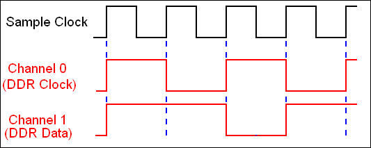
Figure 1. DDR Generation with a Second Clock
Generating DDR at High Speeds
The timing flexibility of NI digital waveform generator/analyzers allows you to generate DDR data at higher rates using a simple circuit on the connector block to combine two digital output channels into a single DDR channel. The NI 6541, 6542, 6544, 6545, 6551, and 6552 devices allows each channel to toggle on the rising edge or falling edge of the sample clock. To combine the two digital output channels complete the following steps:
- Configure one channel to toggle on the rising edge of the sample clock.
- Configure the adjacent channel to toggle on the falling edge of the sample clock.
- Send these two channels to the inputs of an XOR gate.
The resulting signal from the XOR gate output can toggle on both edges of the sample clock.
In Figure 2, channel 0 is configured to toggle on the rising edge of the sample clock, and channel 1 is configured to toggle on the falling edge. Any time either of the two channels toggles, the output of the XOR gate also toggles, creating a DDR signal.
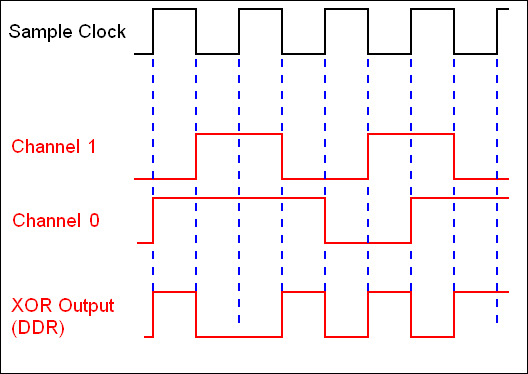
Figure 2. Creating DDR with XOR Logic
An XOR gate is perfect for this application because this simple logic gate allows both inputs to change the output at any time, regardless of the state of the other input. An AND gate, for example, would not work in this situation because either channel can “hijack” the gate’s output—if channel 0 were low during several clock cycles it would prevent channel 1 from changing the output.
Since your data must be split into two channels, some data processing is necessary to convert the desired DDR data into two SDR channels prior to generation. The data processing is simple to understand conceptually. The steps are as follows:
- Assign two channels to be the “rising edge” and “falling edge” channels.
- Looking at the timing diagram from Figure 2, choose the first sample for the two inputs of the XOR gate, based on the initial state of the DDR output. Since the DDR output starts at a logic low in the figure, this example uses logic low as the initial states for both channels.
Figure 3 shows the first samples of channels 0 and 1.
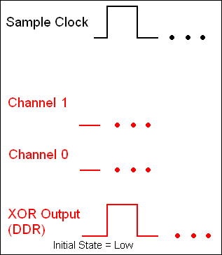
Figure 3. Setting the first samples for the Channels
3. After the initial state, find the next edge of the DDR output and observe the clock edge on which the DDR output edge occurred. If the DDR output edge occurs on the rising edge of the sample clock, then the “rising edge” channel should toggle at that time. If the edge occurs on the falling edge of the clock, the “falling edge” channel should toggle.
Figure 4 shows this procedure for the first two edges of the desired DDR signal.
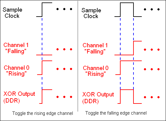
Figure 4. Creating Edges to be Used by the XOR Gate
4. Repeat this process for the duration of the waveform.
The result of this data processing should produce two channels that create the desired DDR output when they are used as inputs to an XOR gate.
While the concept behind the processing is straightforward, its implementation is slightly more complicated and is outside the scope of this document. An example LabVIEW VI is attached to this document which will process a waveform, breaking each channel into the two-component channels to be used as inputs to the XOR gate. A description of the VI operation is included in the VI documentation, which you can access by selecting File>> VI Properties >>Documentation from the LabVIEW menu.
Circuit Description and Schematic
Figure 5 shows a schematic of the simple circuit you must construct on the connector block for a single DDR channel. Since the NI 6541, 6542, 6544, 6545, 6551, and 6552 devices can generate data at speeds up to 100 MHz, the XOR gate must have a propagation delay of less than 5 ns. NI recommends the Fairchild NC7SZ86 (www.fairchildsemi.com), which has a propagation delay of 3 ns (typical) at Vcc = 3.3 V.
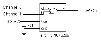
Figure 5. XOR Circuit diagram
C1 should be placed very near the XOR gate to help stabilize the power supply during data transitions. The recommended value for C1 is 0.1 μF. If multiple DDR channels are required, the circuit shown above can be repeated for each additional channel, including one 0.1 μF capacitor for every XOR gate. Another capacitor should be added to the PCB with a recommended value of 10 μF. This capacitor can be placed near the incoming power rails on the PCB, and it will help stabilize the power supply for the entire board.
Software Implementation
Once you have processed the waveform as discussed above, you can easily program the NI 6541, 6542, 6544, 6545, 6551, and 6552 devices to generate the DDR data by completing the following steps:
- Open the Dynamic Generation example program. You can find the example in LabVIEW by going to the Help menu and choosing “Find Examples.” Once the example finder has opened, browse to Hardware Input and Output >> Modular Instruments >> NI-HSDIO >> Dynamic Generation.
- You will need to add two VIs to the program.
- Add niHSDIO Configure Data Position. By default, every channel toggles on the rising edge of the sample clock. Therefore, any channel that must toggle on the falling edge must be configured to do so by this VI. In this example, channel list should be 1, and position should be set to Sample Clock Falling Edge.
- You will also need to add the niHWS Retrieve Waveform VI to retrieve the waveform you previously created.
Figure 6 shows where to insert these two VIs into the example.
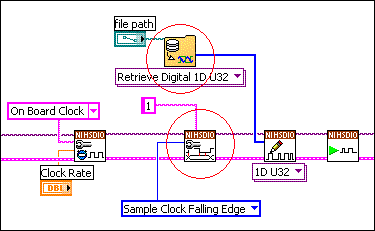
Figure 6. Modifications to Example Program
Once the above modifications are made, the VI is ready to generate your DDR signals.