Higher Current
To deliver higher current, two NI PXIe-4138/9 devices must be connected in parallel so that each can deliver half the current to the load. In constant current (current-controlled) mode, simply program each device to deliver half the total desired current. In constant voltage (voltage-controlled) mode, you must take measures to ensure that the current is shared evenly between the two devices. Even if you configure the devices to source current, they can enter constant voltage mode if they reach the voltage limit. For more information about constant voltage mode and constant current mode, refer to your NI-DCPower Help documentation.
To connect two devices in parallel in constant voltage mode, some positive resistance must exist between them. This limits the amount of current that flows from one to the other due to accuracy mismatch.
For example, suppose your application requires the delivery of 5 V at 5 A using an NI PXIe-4139. Each NI PXIe-4139 device can deliver only 3 A continuously at 5 V, so two modules must be connected in parallel to reach the required 5 A. The goal is to have each source measure unit (SMU) deliver half of the total current. However, because the modules are operating in voltage-controlled mode, they won’t necessarily provide exactly 2.5 A. If the output of one of the modules reaches the 3 A limit, it will enter current-controlled mode. This can cause the system to become unstable and result in an unpredictable output to the device under test (DUT). This situation can be avoided by adding resistance between the two modules to prevent the current limit from being reached.
Assume you decide to limit the current coming from each module to 2.5 A ± 0.2 A. This keeps the current delivered by either SMU comfortably under its 3 A limit. The voltage accuracy specification for the NI PXIe-4139 states that the output voltage is within 0.02% + 300 uV of the programmed value in the 6 V range within 5 °C of the last self-calibration. For a 5 V setpoint, the accuracy works out to be ±(0.02/100 * 5V + 300uV) = ± 1.3mV. The worst-case situation would have one device 1.3 mV high while the other is 1.3 mV low, resulting in a 2.6 mV difference between the two outputs. To limit the current flowing from one device to the other (instead of the load) to 200 mA, you need resistance of 2.6 mV/200 mA = 13 mΩ between the two outputs. Less resistance could work, but if too much current flows between devices you waste power and possibly force channels into compliance prematurely.
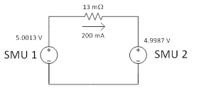
Figure 1. Two parallel devices with slightly different outputs are connected with no load. 200 mA flows from one device to the other.
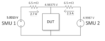
Figure 2. Two parallel devices with slightly different outputs are connected at full load. 2.7 A flows from one and 2.3 A flows from the other.
If you are using local sense, no additional resistance is needed because there is at least 6.5 mΩ of resistance in your interconnect wires, so the two devices can be directly connected in parallel. In this case, though, the voltage at the load is below the programmed value by an amount determined by the load current and the wiring resistance.
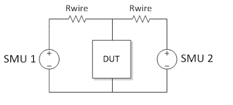
Figure 3. Two parallel devices are configured for local sense with wire resistance shown.
To use remote sense, you need to add explicit resistance between the remote sense connection points and the DUT. This could be in the form of interconnect wire or very low value resistors. If you are using the NI PXIe-4139, you could use its programmable resistance feature to set an output resistance of 6.5 mΩ. (Programmable output resistance is not available on the NI PXIe-4138.)

Figure 4. Two parallel devices are configured for remote sense with added resistors.
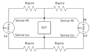
Figure 5. Two parallel devices are configured for remote sense with programmed resistance. (PXIe-4139 only)
The drawback of the resistance is that the voltage at the load is not precisely equal to the programmed voltage—some is lost across the resistance. In this example, the voltage loss is 6.5 mΩ * 2.5 A = 16.25 mV at full load current. However, this is less than the voltage loss experienced with a local sense connection.
Higher Voltage
To deliver higher voltage, two NI PXIe-4138/9 devices must be connected in series so that each can deliver half the voltage to the load. In constant voltage (voltage-controlled) mode, simply program each device to deliver half the total desired voltage. In constant current (current-controlled) mode, you must take measures to ensure that the voltage is shared evenly between the two devices. Even if you configure the devices to source voltage, they can enter constant current mode if they reach the current limit. For more information about constant voltage mode and constant current mode, refer to your NI-DCPower Help documentation.
To place two devices in series in constant current mode, some resistance must exist across each one. This limits the amount of voltage mismatch between the two modules that results from accuracy mismatch.
For example, suppose you wish to source 1 mA with a limiting voltage of ±100 V. Each NI PXIe-4138/9 device can provide only 60 V, so two must be placed in series to reach the required 100 V. The goal is to have each SMU deliver half of the total voltage. However, because the modules are operating in current-controlled move, they won’t necessarily split the total output voltage evenly. If the output of one of the modules reaches its 60 V limit, it will enter voltage-controlled mode. This can cause the system to be unstable and result in an unpredictable output to the DUT. This situation can be avoided by adding resistance across each module to prevent the voltage limit from being reached.
Assume you decide to limit the voltage across each module to 50 V ± 5 V. This keeps the voltage delivered by either SMU comfortably under its 60 V limit. The current accuracy specification for the NI PXIe-4139 states that the output current is within 0.03% + 60 nA of the programmed value in the 1 mA range within 5 °C of the last self-calibration. For a 1 mA setpoint, the accuracy works out to ±(0.03/100 * 1 mA + 60 nA) = ± 360 nA. The worst-case situation would have one device 360 nA high while the other is 360 nA low, for a 720 nA difference between the two outputs. That current drives the common node between the two SMUs, and if you wish to limit the voltage error of the middle node to 5 V to ensure each device stays comfortably within its compliance limits, you need a resistance of 5 V/720 nA = 7 MΩ at the junction of the two devices. More resistance could work, but too much voltage difference between the two devices could force channels into compliance prematurely and waste power in some instances.
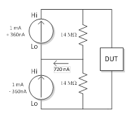
Figure 6. Two series-connected devices with slightly different outputs are connected with parallel resistors.
The configuration shown in Figure 6 has the bottom SMU providing current not only to the load, but also to drive the common-mode capacitance of the top SMU. This can result in long settling times as that capacitance is slowly charged. You can address the problem by reversing the connections of the bottom SMU as shown in Figure 7. This necessitates reversing the sign of its programmed current.
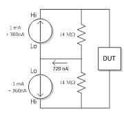
Figure 7. Two series-connected devices share Lo to reduce loading from common-mode capacitance.
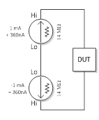
Figure 8. Two devices are connected in series with programmed parallel resistance. (NI PXIe-4139 only)
The drawback of the added parallel resistance is that the current delivered to the load is slightly less than the programmed value, because some goes to the resistors. In this example, the current loss is 50 V/14 MΩ = 3.6 uA at full load voltage.
In some situations, you may need to source current with a unipolar compliance limit. For example, suppose you want to source 1 mA into a voltage that can vary from 0 V to +100 V. In that case, you can use one SMU to offset the second by 50 V. The first SMU would be set to 50 V in voltage mode with a current limit higher than the desired 1 mA. The second SMU is configured for 1mA with over a 50 V limit to ensure that it can swing from 0 V to 100 V. The DC offset from the first SMU allows the second SMU outputting -50 V to +50 V to result in a voltage of 0 V to +100 V across the DUT. There is no need for resistors, because the voltage of the junction of the two SMUs is defined by the first SMU. Because there are no extra resistors, there is no additional current loss.
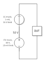
Figure 9. With these two series-connected devices, the bottom is configured for 50 V with 10mA limit and the top is configured for 1 mA with 55 V limit. The junction voltage is 50 V.
Choosing between Series and Parallel Operation
Consider a situation in which you want to generate 15 V at 2 A to power a device. This 30 W requirement is beyond the 20 W continuous power delivery envelope of a single NI PXIe-4139. You could parallel two devices to deliver 1 A each at 15 V. This would require the external balancing resistors mentioned above. Alternatively, you could connect two modules in series, each delivering 7.5 V at 2 A. This option doesn’t require any external balancing resistors and is therefore preferred. However, because there are no balancing resistors, you should consider what can happen if the current limit is reached. In this case, it is best to let the module on top reach its current limit before the bottom one to prevent a common-mode voltage swing on either SMU. The bottom device could be set to 6 V with a current limit of 3 A while the top device is set to 9 V with a current limit of 2 A. The output of each device is within the 20 W power limit, but only the top device is able to reach its current-limit.
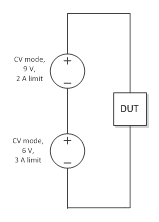
Figure 10. Here are two series-connected devices with different voltage levels and current limits.
Synchronization
When connecting multiple SMUs in parallel or series, it is important to synchronize the outputs with the same—or similar—configuration properties. This maintains the desired balance of each SMU and prevents cross driving. Synchronization becomes especially important when operating in sequence source mode.
To synchronize two SMUs, you need to define one SMU as the master and the other as the slave. The master SMU is responsible for signaling the slave SMU to initiate and to advance to the next sequence step. All signaling is done using the events and triggers available through the NI-DCPower driver.
In the next section, learn how to synchronize multiple NI PXIe-4138/9 outputs for a sequence of setpoints and a sequence of pulses.
Sequence of Setpoints
The first step to synchronize your devices is to make sure that both devices’ initial states are the same. Not only should they be programmed to reach the same configuration, but they should also start in the same state. If one device starts in a different state, it could add additional delay or possibly source into the second device before it is ready.
To ensure that both devices are in the same initial state, add an initial sequence step with both voltage and current set to zero. Then program subsequent steps with identical properties for both devices—such as voltage level/limit, current level/limit, operating range, and so on. This prevents one SMU from driving the other SMU into compliance and keeps both devices in sync.
After configuring both devices, make sure the slave device is ready to receive a trigger before the master device sends one. To achieve this, initiate the slave device before initiating the master device. Initiating the devices in this order prevents triggers from being lost.
When the master device is initiated, it sends a Start Trigger to the slave device, which begins executing its respective sequence. If the master and slave sequences are programmed with identical source delays and aperture times, both devices will finish outputting each setpoint at almost the exact same time. If the slave finishes slightly after the master, the trigger from the master could arrive before the slave is ready for it causing the two devices to lose their synchronization. To prevent this from happening, add a measure complete event delay in the master, which gives extra time to the slave to finish its execution before the master trigger is sent.
This master-slave coordination for a sequence of setpoints is depicted below.
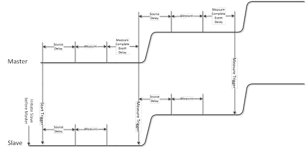
Figure 11. Two sequences of setpoints are synchronized by using a Measure Complete Event Delay.
You can add a Measure Complete Event Delay using an NI-DCPower property node. The duration of this delay depends on your master-slave setup—for example, how far the slave and master are from each other. In internal tests a 1 ms delay was sufficient. For performance purposes, this delay can be considerably decreased if the system is properly characterized.
If you are only sourcing and not measuring, instead of adding a Measure Complete Event Delay, just decrease the Source Delay in the slave to make sure that the slave is ready for the master. A simple approach is to multiply the master source delay by a coefficient less than 1, and use the result as the source delay for the slave device.
It is important to consider that each device returns its own measurements. To have a combined voltage/current measurement, you need to combine the respective device’s measurements inside your specific application.
For the series-connected case, add up the voltage measurements coming from each device and average the current measurements. If the circuit has one SMU reversed as shown in Figures 7 and 8, then remember to negate the values returned from that SMU before combining them with values from the other SMU. For the parallel-connected case, add up the current measurements and average the voltage measurements.
Now that you have analyzed how to sync a single sequence step, you can repeat this pattern with all the following sequence steps.
Sequence of Pulses
Configuring a sequence of pulses is conceptually similar to configuring a sequence of setpoints. You still need to initiate the slave device before you initiate the master device so the slave device is ready for the master Start Trigger. You also need to ensure that the initial state and configuration are the same for both devices. You should add in a step at the beginning of your sequence with the voltage/current set to zero. This step ensures one SMU does not start sourcing while the other one is still getting ready (closing its output relay, for example). Finally, you need to appropriately time your trigger signals so that the slave is ready for every pulse trigger the master sends.
Different events and triggers are used to signal between the slave and master devices when synchronizing a sequence of pulses. Also, the off time attribute should be used to determine when master device sends its Pulse Trigger to the slave.
In Figure 12, the slave is ready to receive the Start Trigger from the master before the master even starts. Then both devices update their output and take their respective measurements synchronously before going back to their bias levels. Finally, the slave device has a shorter off time than the master so it is ready to receive a Pulse Trigger from the master device.
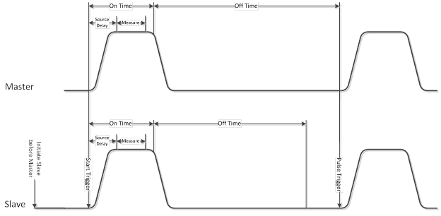
Figure 12. Two sequences of pulses are synchronized by decreasing the slave’s off time.
A simple approach to determine what off time to use for the slave device is to multiply the master device’s off time by a coefficient less than 1. This coefficient can vary depending on the value of the off time for the master device. In internal tests, 0.9 was a sufficient value for this coefficient. In general, you should make sure that the slave off time is greater than the slave pulse bias delay (the delay before the pulse returns to its bias level).
Out-of-range pulsing is supported by the NI PXIe-4139 SMU only.