Interfacing NI DAQ TTL and CMOS Circuits

Updated Feb 22, 2023

Environment

Other

  • External Buffers and Circuitry

The difference between TTL and CMOS signals can be described by the following:
  • CMOS circuits do not draw as much power as TTL circuits while at rest. However, CMOS power consumption increases faster with higher clock speeds than TTL does. Lower current draw requires less power supply distribution, therefore causing a simpler and cheaper design.
  • Due to longer rise and fall times, the transmission of digital signals becomes simpler and less expensive with CMOS chips.
  • CMOS components are more susceptible to damage from electrostatic discharge than TTL components.
This article explains how to interface the digital lines on an NI DAQ Board to a CMOS circuit, including how to connect two digital signals with different voltage levels.
 

The following figures demonstrate how to interface a TTL signal to a CMOS circuit and a CMOS circuit to a TTL input. The figures also show how to interface the two circuits if the voltage levels are incompatible.


Figure 1: TTL-to-CMOS interfacing using pull-up resistor


Figure 2: CMOS-to-TTL interfacing using a CMOS buffer IC
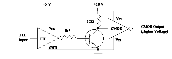


Figure 3: TTL-to-CMOS interfacing using a transistor


Figure 4: TTL-to-CMOS interfacing using a TLL open-collector buffer IC


Figure 5: CMOS-to-TTL interfacing using a CMOS buffer IC

(Roger L. Tokheim, Digital Electronics, 3d ed., McGraw-Hill, New York, 1990)