Introduction
You can use Multisim to create specialized schematics that describe the logic of a PLD, such as the FPGA on the NI Digital Electronics FPGA Board (DEFB). Multisim also includes configurations to automate creating synthesizable and implementable designs for the DEFB.
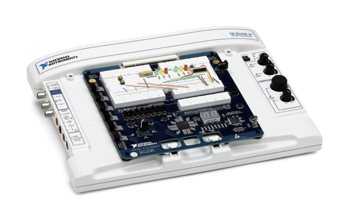
Figure 1. NI Educational Laboratory Virtual Instrumentation Suite (NI ELVIS) II+ and the NI Digital Electronics FPGA Board Top
This article describes the step-by-step process, from DEFB creation to programming, using Multisim and Xilinx ISE Tools. As a test design, you can implement simple OR logic using two switches and one LED on the DEFB. Again, you can use a similar process to program other FPGAs.
Follow these three steps:
- Create a new PLD design in Multisim
- Describe the logic in Multisim
- Export digital logic
Required Software and Hardware
- NI Multisim 12.0
- External Link: Xilinx ISE Tools 13.x, 12.x, or 10.1 SP1
- NI Digital Electronics FPGA Board 3.1 or later driver software
- NI Digital Electronics FPGA Board
Note: You may use earlier versions of Multisim with earlier versions of Xilinx ISE Tools. Verify the version compatibility in the release notes for earlier releases of Multisim.
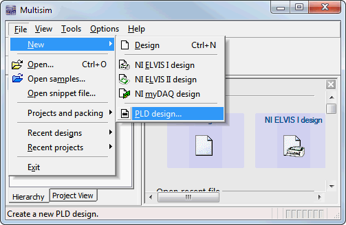
Step 1: Create a New PLD Design in Multisim
The first step is to create a new PLD design in Multisim. In this example, use the standard configuration for the DEFB. This configuration file is configured to automatically map Multisim signals to the appropriate pins on the FPGA.
- Open Multisim 12.0 and navigate to File»New»PLD Design…
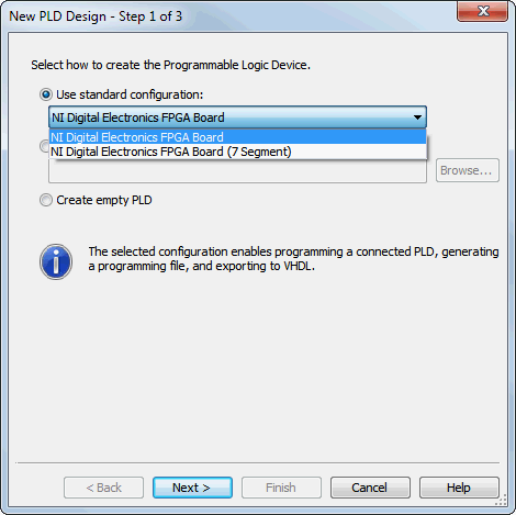
- Select Use standard configuration and ensure that Digital Electronics FPGA Board or NI Digital Electronics FPGA Board (7 Segment) is selected. They are the same FPGA target, but the 7-Segment version has a 7-Segment LED populated on the board as an indicator. Select Next to proceed.
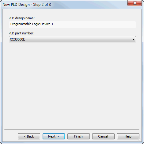
- Modify the PLD design name as desired. The PLD part number should always be XC3S500E because this is the Xilinx FPGA that is used on the DEFB.
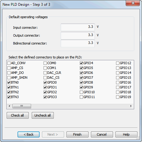
- Select the desired simulation parameters for the Default operating voltages. Note that these do not affect the physical device, and they are used only for simulation. Toggle any predefined connectors that you would like to have available in Multisim when designing the FPGA logic; for this example, just leave the default selections. Select Finish to create the PLD schematic with the inputs and outputs populated.
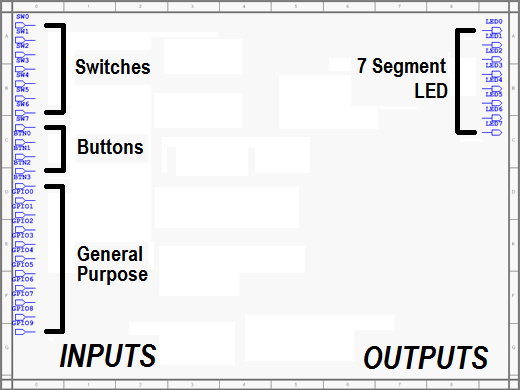
- The PLD schematic appears with all inputs on the left-hand side and all outputs on the right-hand side as shown in the figure below. You are now ready to add logic to the PLD schematic.
Step 2: Describe the Logic in Multisim
The next step is to describe the logic for the OR gate.
- Right-click the diagram and select Place Component…
- Use the following parameters in the Select a Component (PLD Mode) window
Database: Master Database
Group: PLD Logic
Family: Logic Gates
Component: OR2
The OR2 component is an OR gate with two input pins. In the same manner, an OR8 component is an OR gate with eight input pins.
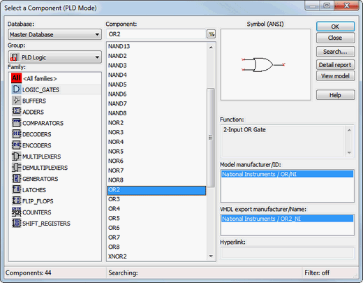
Select OK to place the component on the diagram. This positions the OR2 gate on the clipboard, so it is ready to be placed on the schematic. Left-click to place the OR gate to the right of SW0 and SW1.
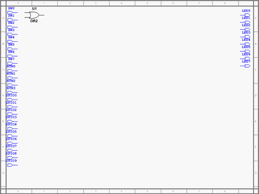
- Move LED0 just to the right of the OR2 gate and wire the output of the OR2 gate to the input of LED0. Then wire the output from SWO and SW1 to the inputs of OR2. The completed logic appears as shown in the figure below. You are now ready to export your digital logic.
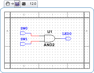
Figure 2. Multisim PLD Design Snippet: Drag and
drop into Multisim 12.0 or later to import logic.
Step 3: Export PLD Logic
To export the digital logic, navigate to Transfer»Export to PLD...
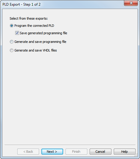
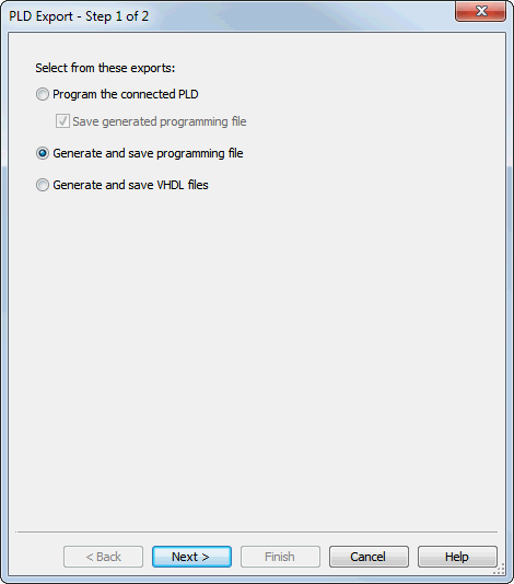
You can choose from three options to export the PLD logic: (1) program the connected PLD with the option to save the programming file (if the PLD is connected and detected), (2) generate and save the programming file, and (3) generate and save VHDL files. All three have unique benefits, which are explained further in the next three sections.
Program the Connected PLD
The benefit to programming the connected PLD is that it allows you to validate the digital logic with hardware, providing immediate results. The drawback is that you must connect the hardware to the computer for programming.
The following procedure outlines how to program a connected DEFB.
- Select Program the connected PLD as shown in the figure below. Choose to Save the generated program file if this is desired. If you do this, you can reuse the program file in the future, which will save you time. Select Next to proceed.
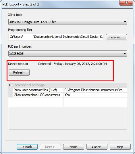
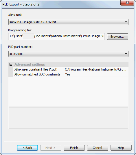
- Choose the Xilinx tool to compile the Multisim PLD design to a programming file. If you installed the Xilinx ISE Tools to the default location, they should autopopulate. If not, click the Xilinx tool drop-down menu and select Manually select tool and then browse to the file folder where the tools were installed. The Xilinx user constraint file contains directions that map the connectors in Multisim to the pins of the Xilinx FPGA, Part Number XC3S500E.
- At this point, you must connect the DEFB to your computer. Ensure that the board is powered on using the switch on the board and that it is connected to the PCI connector of an NI ELVIS II board that is connected to the computer via USB. To check if all requirements have been met and the device is properly connected to Multisim, click the Refresh button. If the board is detected, the Device status displays Detected - Date and Time, as shown below.
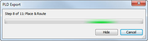
- To proceed, click Finish. This begins the 11-step process of programming the PLD. Multisim automatically invokes the Xilinx ISE Tools (Creates the Xilinx project, Checks syntax, Translates, Places & Routes, Generates the programming file, and so on), and then you can program the connected Xilinx Spartan 3E FPGA on the DEFB. You can monitor progress from the modal window, as shown below, and find a more detailed report in the Spreadsheet View of the Multisim environment.
- After you have successfully programmed the PLD, you can toggle the switched SWO and SW1 to observe when LED0 is illuminated and confirm the functionality of the two input OR logic gates on the DEFB.
Generate and Save Programming File
If hardware is not immediately available and the end goal is to deploy to an FPGA, you can generate and save a programming file targeted for an FPGA. This file is the closest step to actually programming the physical FPGA, allowing a student to bring the programming file to class and quickly deploy to the FPGA to get results using the Xilinx ISE Tools. The following procedure outlines how to generate a programming file using a Multisim PLD export:
- Select Generate and save programming file as shown in the image below. Select Next to proceed.
- Choose the Xilinx tool to compile the Multisim PLD design to a programming file. If the Xilinx ISE Tools were installed to the default location, they should autopopulate. If not, click the Xilinx tool drop-down menu, select Manually select tool, and browse to the file folder where the tools were installed. The Xilinx user constraint file contains directions that map the connectors in Multisim to the pins of the Xilinx FPGA, Part Number XC3S500E.
- Select Finish to proceed through a nine-step procedure; two steps are removed for detecting the hardware and programming the hardware because they are not required.
Generate and Save VHDL Files
At the culmination of most introductory digital logic courses, students are introduced to hardware description languages (HDLs). A powerful feature of the PLD schematic is the ability to generate VHDL code from the PLD logic in Multisim. Using Xilinx ISE Tools, students dive deep into VHDL and add critical timing constraints to the generated VHDL code when required. The following procedure outlines how to export the digital logic to VHDL in Multisim.
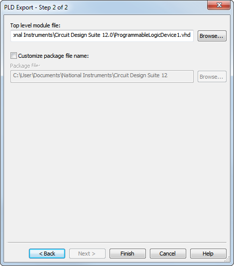
1. Select Generate and save VHDL files as shown in the image below. Select Next to proceed.

2. Select the name of the Top level module file. You may also specify if you prefer to Customize package file name. If you do not specify this, Multisim appends _pkg to the end of the specified top level module name. Select Finish to generate the files.
3. You can now open and explore the resulting VHDL files as well as import them into Xilinx ISE Tools to add timing constraints.
Conclusion
Multisim continues to provide a best-in-class teaching solution for circuit theory, including Digital Logic, with the continued support for Xilinx FPGA tools. The PLD schematic offers a graphical environment to better understand the fundamentals of digital gates, and then smoothly transition to more advanced concepts such as combinatory logic, and finally, students can explore VHDL and program PLDs.