Noise Analysis
Noise Analysis is a small signal analysis which is carried out at discrete frequencies using a linearized version of the circuit. The mechanics are very similar to those of an AC analysis. The key difference is that in AC analysis the signal generators are AC signal sources explicitly defined by the user whereas in noise analysis the signal generators are invisible noise sources attached to every noise-generating element in the circuit, such as to the resistor shown below:
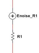
Figure 1: Noise model of a simple resistor
Additionally, in AC analysis the AC signal source amplitude and direction are set explicitly by the user while in noise analysis the amplitude of the noise source is set through a formula representing the physical noise phenomena of the noise-generating element. The noise generators within the circuit are completely uncorrelated and therefore have no direction; their additive effect on any circuit node is calculated in an RMS-manner.
Note that unless explicitly modeled by the user, noise originating externally to the circuit (e.g from a previous stage in a signal chain) is not injected or modeled by Noise Analysis. For example, AC sources do not inject any noise into the circuit; all voltage sources are shorted and all current sources are open-circuited.
Noise generators
Every resistor and every semiconductor device in the circuit has at least one noise generator associated with it. While plain resistors only generate thermal noise, semiconductors may generate thermal, shot, and Flicker noise. Op-amp and precision reference components typically use macro-modeling techniques to synthesize white and 1/f noise (this is discussed later).
Setting Noise Analysis Parameters
Analysis parameters tab
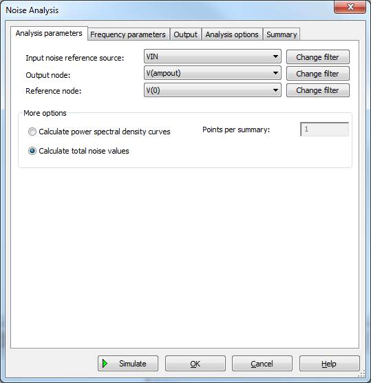
Figure 2: Analysis parameters dialog
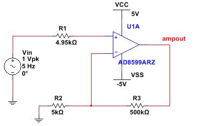
Figure 3: Sample circuit for noise analysis
Output node:
This is the node for which the noise calculations will be made. In the above example it is ampout on our circuit.
Reference:
This node acts as the reference to the output node. This is set to V(0), which is ground if the noise calculation is single-ended (relative to SPICE ground node 0). It is set to any other node for a differential noise calculation.
Input noise reference source:
You must specify a reference voltage or current source for input-referred noise calculations. Input-referred noise and voltage noise on the circuit output node are related through the small-signal gain between the reference source and output node.
As specified in Figure 2 for the circuit in figure 3, the input-referred noise and the output noise are be proportional through the small-signal gain of 100 (R3/R2) in low frequencies. Note that even though the input-referred noise may not be of interest to you, specifying a reference source is a requirement of the simulator.
Also note that this source is not a noise source as it does NOT inject noise into the circuit and is therefore removed during the calculations of noise contribution. During this calculation, all non-noise generating voltage sources are shorted and current sources are open-circuited. As such an equivalent circuit is generated by the simulator (as shown in Figure 4) which shorts the source Vin and moves it to some unrelated location thereby having no impact on the output noise calculations.
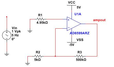
Figure 4: Equivalent circuit for calculating output noise
Calculate power spectral density curves
This option instructs the simulator to generate power spectral density curves across the frequency range configured in the Frequency Parameters tab. The Points per summary option down-samples the number of points that are used for the curves. It is recommended to leave it at 1.
Calculate total noise values
This instructs the simulator to integrate power spectral density curves and generate a total noise value. The result is single scalar value representing the area under the power spectral density curve for the frequency range specified in the Frequency parameters tab. In effect, the result is the noise voltage that would be experienced by the circuit if the circuit were somehow perfectly limited to the specified frequency range (or bandwidth).
Note that for both the spectral density curve option and total noise option, the simulator generates noise power, not RMS noise. If you need to convert to RMS noise (e.g to get a reading in V/√Hz), you can create an expression within the grapher application and use the sqrt()function to take the square root.
Frequency parameters tab
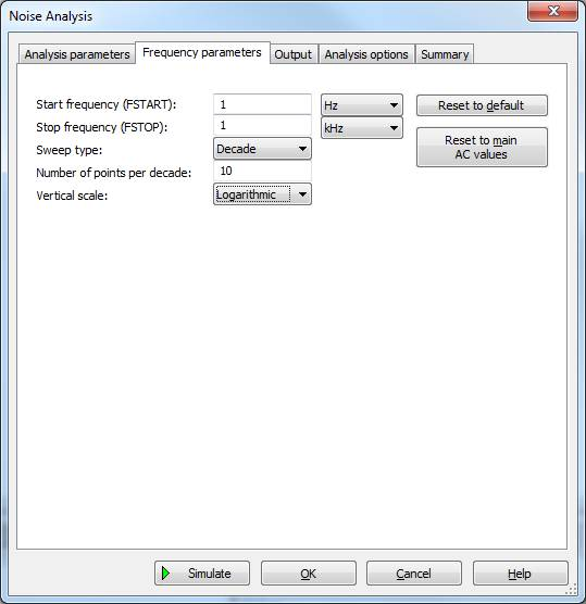
Figure 5: Noise analysis setup
This tab is used to set the frequency range across which the analysis is carried out. Unless using the Calculate total noise values option to integrate the noise density between two frequencies, it is recommended to carry out the analysis across a wide range – much wider than the inherent bandwidth of the analyzed circuit (this is the same idea as when running regular AC analysis).
Output tab
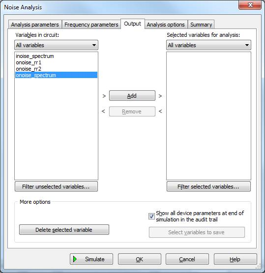
Figure 6: Noise analysis setup
This tab lists and allows you to select from various outputs that can be generated and reported by the analysis.
Output node voltage noise vs. Input referred noise
Output variables that are prefixed with onoise such as onoise_rr1 refer to voltage noise produced on the circuit output node. Output variables that are prefixed with inoise such as inoise_total_rr1 refer to input-referred noise at the input reference source. Input-referred noise and voltage noise on the circuit output node are related directly through the small-signal gain from the reference source to the output node.
Typically, it is voltage noise produced on the output node that is of greater interest.
Total noise
The output variable name that designates the total noise from of all noise generators in the circuit is:
- onoise_spectrum, if you are using the spectrum density option
- onoise_total, if you are using the total or integrated noise option
In the majority of cases, the total output variables are the most important because they represent the noise that the output node will experience in real life.
Individual contributors
Noise analysis can also show the contribution from each individual noise source to the total noise. The contributing noise source can be deduced from the output name. For example, onoise_total_rr1 refers to the contribution from the thermal noise associated with resistor R1; while onoise_total_dd1_1overf refers to the contribution from the 1/f noise (or Flicker noise) associated with diode D1; and onoise_total_dd1 refers to the contribution from all noise sources associated with diode D1.
It is important to understand that these output variables do not represent the value of the noise generator but rather the noise generator’s contribution to noise on the output node.
It is also good to understand that, in and of themselves, many of these output variables are meaningless. This is because SPICE macro-models, such as those used to model op-amps, use elements such as resistors and diodes to synthesize some higher-order or macro behavior. For example, op-amp macro models may use diodes as part of a current limiting function. These diodes have no meaning to the noise effects being modeled, yet their contribution may still show up as an output variable in Multisim (of course if the op-amp model is designed to simulate noise, the contribution from these elements should be negligible).
Noise in op-amps and in other models
Noise Analysis is commonly applied to circuits containing op-amps. Many models of op-amps that are designed for precision applications include an internal noise model, which typically takes the form of voltage and current noise generators at the input terminals. However, not all op-amp models include a noise model. It is prudent practice for the model user to verify whether or not noise is modeled. The methods below outlines some of the ways of accomplishing this.
- Inspect the comments in the SPICE model
SPICE model designers often leave useful comments for the user within the SPICE model. Click the View model from the component browser.
Useful comments may be found in the model header as shown below.
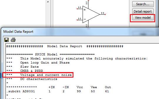
Figure 7: Noise modeling in SPICE components
Useful comments may also be found within the body of the actual model. For example
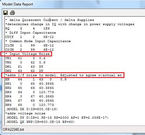
Figure 8: Noise modeling in SPICE components
- Look for the Flicker coefficient parameter KF
Model designers frequently use the Flicker noise behavior of semiconductor device models (typically diodes) to macro-model the 1/f noise of op-amps. The parameter ‘KF’, named the Flicker coefficient, affects the Flicker noise equation directly. With its default (or unspecified) value of zero, semiconductor device models, or anything else modeled using those device models, do not exhibit Flicker noise. Therefore, if a device model contains the parameter ‘KF’ on the .model line and it is set to some non-zero value, it is an indication that noise is very likely modeled.
The best way to determine whether or not noise is modeled is to test the op-amp model and compare the results against the datasheet, which specifies voltage and current noise density curves referred to the inputs terminals of the op-amp.
Let us consider testing the Analog Devices AD8599 model as an example. The following voltage noise density and current noise density curves are provided in the datasheet:
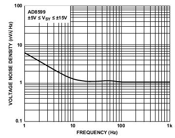
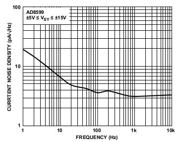
Figure 9: 1/f Noise as specified in component datasheet
Set up a simple voltage follower configuration, as below.
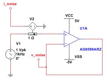
Figure 10: Configuration for testing op-amp noise. V2 is an ideal current-controlled voltage source. It is used to sense the noise current flowing into the non-inverting terminal and report it as a voltage on node I_noise. V1 is the reference source. It is required by the simulator.
To extract the voltage noise density curve, set Noise Analysis to calculate power spectral density curves, set the frequency range to 1Hz to 1kHz (same as in datasheet), set the v_noise node as the output node and graph the onoise_spectrum output variable, which represents the power density on node v_noise.
Note that the output variable represents noise in V2/Hz, not V/√Hz. To convert the result to the latter, add a trace with the expression sqrt(onoise_spectrum) within the graph using the “Add Traces..” command.
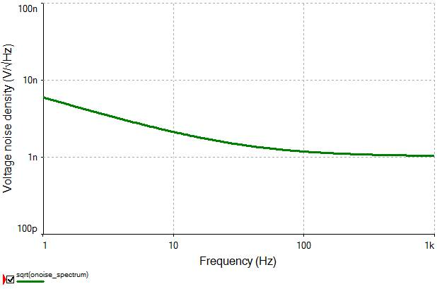

Figure 11: Toolbar command for adding new traces and expressions
The results match up with the datasheet quite well.
In this case the op-amp has non-negligible current noise, which may turn into non-negligible voltage noise if it passes through significant impedance. Therefore, it is good to ensure that current noise is modeled as well. To extract the current noise density curve, simply change the output node to I_noise and re-run the analysis between 1 and 10kHz. To convert the result A/√Hz, add a trace with the expression sqrt(onoise_spectrum) .
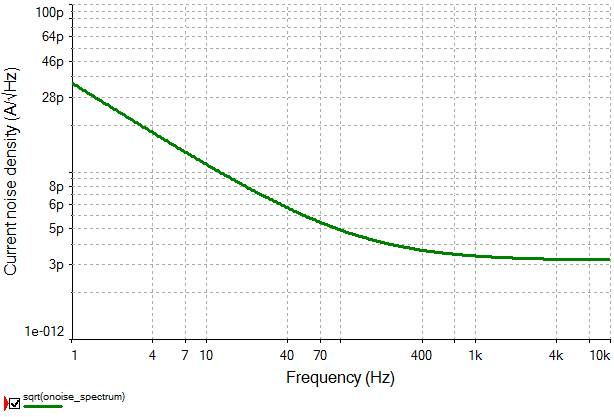
Figure 12: 1/f Noise in Multisim
The overall results match up quite well with the datasheet, white noise in particular.
Now that we have gained confidence in our model, we are ready to apply it to a practical problem.
Practical problem
Let us assume that there is a slowly-varying (<5Hz) input signal with a voltage range of 60mV which needs to be amplified and digitized. The requirement is determine whether or not the circuit in Figure 7, in combination with a 16-bit A/D, achieves a Signal-to-Noise (SNR) ratio of 100dB after the amplified signal is digitized. If does not achieve this specification, then a noise filter should be added such that it does.

Figure 13: Amplification circuit
With the amplifier gain of 100, the output signal has a range of 6V. The RMS voltage noise, Vn_Totalrms , corresponding to 100dB and that which must not be exceeded at the A/D input is calculated as follows:


The A/D itself has quantization noise. The quantization noise on a 16-bit A/D operating with the same +5V/-5V supplies is:

Since the A/D quantization noise and the noise from the amplifier circuit, Vn_Amprms, are uncorrelated, they add up as a sum of squares, namely:

Therefore, the maximum RMS voltage noise produced by the amplification circuit is 41 uVrms
At this point, we can use Multisim to determine the noise that this amplifier circuit produces on node Out and see if it is less than 41uV. There are few ways to do this. We can use the Calculate total noise values option in the Noise Analysis dialog. This would provide a scalar value representing the integrated noise across a specified bandwidth. However this information would not provide us with a good indication of how integrated noise is affected by bandwidth, in case we need to make adjustments to the circuit. Therefore, we shall use the Calculate power spectral density curves option and then use some post processing functions to get a better understanding of how noise is affected by bandwidth.
In the Analysis tab, we use the following settings:
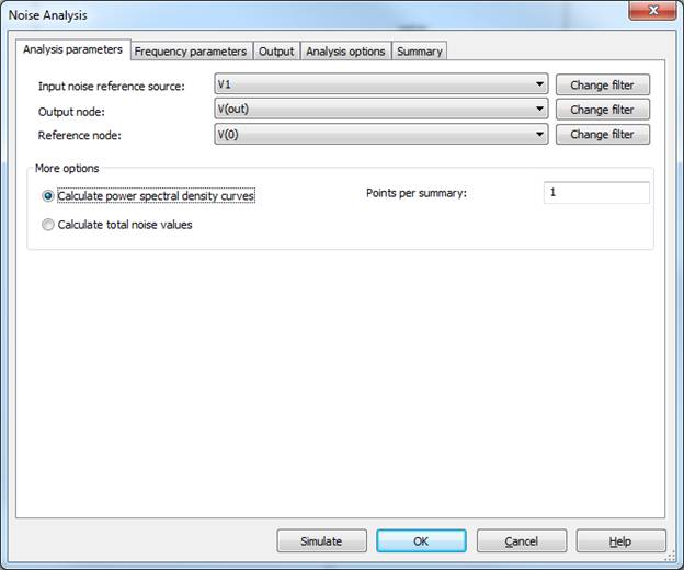
Figure 13: Noise analysis setup
In the Frequency parameters tab, we use the following settings:

Figure 14: Noise analysis setup
The analysis is carried out across a very large bandwidth (0.1Hz to 10GHz) so that we have an entire picture of how the noise varies with frequency.
In the Output tab, we use the following settings:
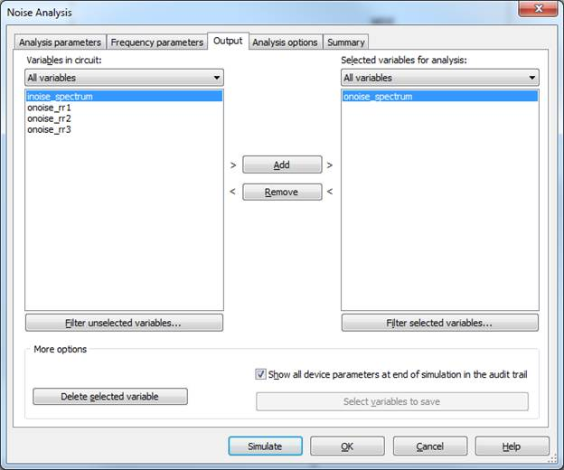
Figure 15: Noise analysis setup
The simulation will be a plot of noise density in units V2/Hz. However, we are looking for an integrated noise plot in units Vrms. To do this, we can create an expression using the integral() function. It will return a plot in units V2, so we simply apply the sqrt() function to get the desired result. The overall expression is sqrt(integral(onoise_spectrum)). The result is shown below.
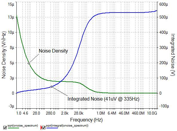
Figure 16: Noise curves before adding a filter stage
The shapes of the curves match intuition. The noise density plot is high at very low frequencies as a result of the op-amp’s 1/f noise. At approximately the cut-off frequency of the circuit, the noise density starts to fall, as would all signals in the circuit. The Integrated Noise plot represents the running integral (starting at 1Hz) of the noise density plot. Obviously starting with zero noise for zero bandwidth, the integrated noise climbs quickly, leveling off shortly after the cut-off frequency when little noise is being contributed by each frequency.
Therefore, if no additional filtering is added to the circuit to limit its bandwidth, the Integrated Noise plot shows that there will be approximately 530uV of noise on the output – far above our of required limit 41uV. However the plot shows us that in order to limit the noise to 41uV, the bandwidth should be limited to approximately 335Hz. So let us add-in a simple, buffered R-C filter as follows:
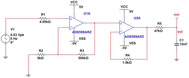
Figure 17: Amplifier circuit after adding an RC filter stage
Please also note that adding the buffer and resistors would introduce noise which are picked up at “out” pin.
The above circuit produces the following noise curves:
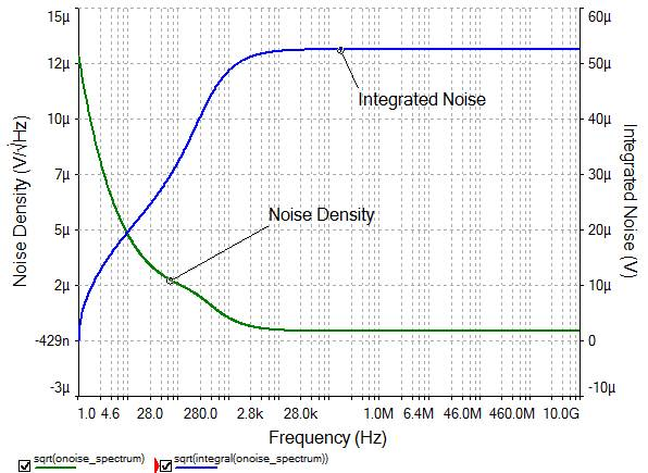
Figure 18: Noise curves after adding a filter stage
Now, the Integrated Noise has leveled off at approximately 53uV – a lot closer to the required 41uV! Therefore we may want to limit the bandwidth slightly more. However proceeding with this would not add any more value to this example, which is meant to illustrate how NI Multisim’s Noise Analysis can be used and why it is such a beneficial tool for the designer.