You will need to export a timing signal from one board and read it with the second board using R Series external timing and synchronization lines. For PCI boards, an external RTSI Bus can be used to connect multiple cards together. For PXI modules, the synchronization bus is built into the backplane of the PXI chassis and is referred to as the PXI trigger bus. You can use the RTSI/PXI trigger bus lines to synchronize an R Series device to any other device that supports RTSI/PXI trigger bus triggers. For both form factors, the synchronization bus can be accessed through FPGA I/O Nodes.
To add a RTSI FPGA I/O to your target:
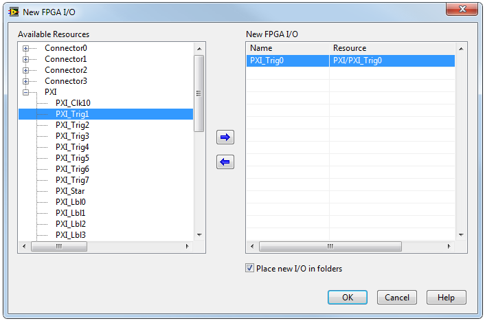
- Right click on your FPGA Target in the Project Explorer window and select New»FPGA I/O.
- Under Available Resources in the New FPGA I/O Window that opens, expand the RTSI or PXI resource (selection will vary depending on R Series device and form factor)
- Select the desired RTSI or PXI_TRIG lines and click the blue right arrow to add the FPGA I/O to your project.
- Click OK.

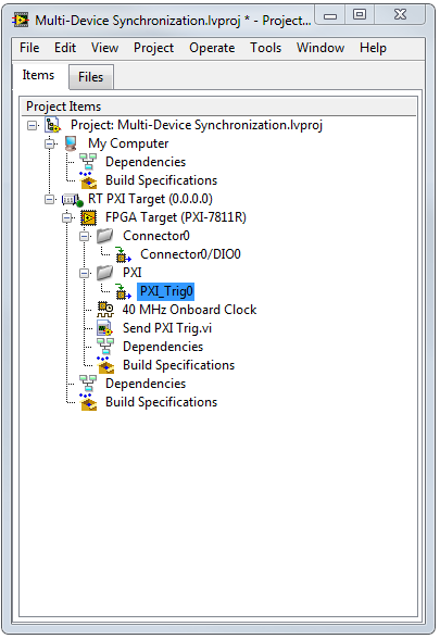
The RTSI/PXI Trigger Bus line should now be displayed in your project under your FPGA Target, as shown below:

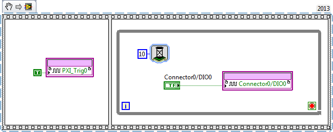
Once added to the project, a RTSI/PXI Trigger Bus FPGA I/O node can be added to the block diagram as shown below. It can be configured as either an input or an output signal, similarly to digital I/O lines. A simple example is shown below, where the PXI Trigger0 line is triggered on a PXI- 7811R prior to the start of a digital write.

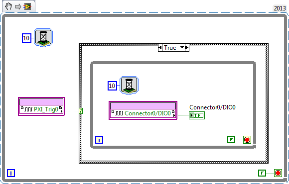
Another R Series card, such as a PXI-7841R, located in the same PXI chassis is then able to read the value on the synchronization bus as shown below. In the example below, the R series card waits for the trigger on the PXI Trigger Bus. Once the trigger is received, the device begins reading from a digital input.

Usually when using relatively low loop rates (kHz range) a drift between the master and slave could exist due to the loops not being in phase. To minimize this drift and improve timing resolution it is recommended to use higher loop rates (MHz range).
Additional Information
The RTSI/PXI Trigger Bus lines are connected in parallel to all other RTSI devices on the bus, and thus only one device should drive a RTSI/PXI Trigger Bus line at a time. You can damage devices by driving the same synchronization line from two different devices.