How to Setup a Multi-Channel Phase Coherent System With PXIe-583x Vector Signal Transceiver

Updated Sep 6, 2023

Environment

Hardware

  • PXIe-5830
  • PXIe-5831
  • PXIe-5832

Software

  • LabVIEW

Driver

  • NI-RFSA
  • NI-RFSG
  • NI-TClk

Multi-channel phase coherent systems are highly considered in several applications, such as Active Electronically Scanned Arrays for Radar, EW, GNSS and 5G networks,  typically for beam steering, multipath signal propagation, estimating channel parameters and testing antenna arrays. For successful beam shaping and scanning in array systems, it is essential to precisely set the amplitude and phase differences between the element channels. However, considerable amplitude and phase differences among those channels can occur due to the RF instrumentation connected to each element. 
In this article we will discuss how we can equalize the phase and amplitude differences between the multi generation/Analysis channels, by building a phase coherent system, based on Vector Signal Transceivers (VST) PXIe 5830/1, covering C/X/K/Ku band, where we will go through the physical system setup and the hardware property settings using the RFSA and RFSG drivers API.


Overview of PXIe-5830/1 architecture:

The PXIe-5830 is an IF vector signal transceiver instrument comprised of the PXIe-5820 and PXIe-3621 while the PXIe-5831 is an IF and mmWave-capable vector signal transceiver comprised of multiple modules, including the PXIe-5820, PXIe-3622, and PXIe-5653 as an optional LO source. Additionally, the PXIe-5831 offers a flexible port arrangement if connected to one or two mmRH-5582 mmWave Radio Heads.

The PXIe-3621 and PXIe-3622 contain an I/Q modulator and I/Q demodulator with wide instantaneous bandwidth to upconvert and downconvert signals from the PXIe-5820 baseband transceiver through differential I and Q ports. The switched IF ports, IF0 and IF1, cover a tuning range of 5 GHz to 12 GHz for the PXIe-3621 and 5GHz to 21GHz for the PXIe-3622.
 

PXIe-5830 IF operation:

The PXIe-3621, part of PXIe-5830, is a full-duplex transceiver with IF0 and IF1 ports. The signal direction on each port, IF0 and IF1, can be reversed to facilitate testing of DUTs with two bi-directional ports. The modules also contains two internal synthesizers, LO2 0 and LO2 1 (for IF0 and IF1 paths respectively), that can be tuned independently thus allowing transmitting and receiving at different tune frequencies. Additionally, a single synthesizer, LO2 0 or LO2 1, can be shared between the I/Q modulator and I/Q demodulator to achieve phase noise cancellation when the transmit and receive tune frequencies are the same, alternatively an external LO can be used on LO2 IN port.


PXIe-5831 IF & mmWave Operations:

The PXIe-3622, part of PXIe-5831, provides the transmit and receive IF signals and LO signals, which are in the X and Ku frequency bands, and are chosen to avoid low-order images and intermodulation products at millimeter wave frequencies. This module contains six IF ports and two LO1 ports (see below picture), from which, two IF transmit ports, two IF receive ports, and two LO1 ports provide connectivity for two mmRH-5582 frequency converters. The remaining two IF ports on the PXIe-3622 are half-duplex ports with a tuning range of 5 GHz to 21 GHz and are used similarly like the IF ports of the 3621 without additional frequency translation. Since the PXIe-3622 is a full-duplex transceiver, one half-duplex port can be used in transmit and the other in receive simultaneously, and the signal direction can be reversed for each port.


Similarly like the 3621, The PXIe-3622 contains an I/Q modulator and I/Q demodulator with wide instantaneous bandwidth to upconvert and downconvert signals from the PXIe-5820 baseband transceiver through differential I and Q ports. Additionally, there are four synthesizers inside the PXIe-3622. Two synthesizers, connectors LO1 0 mmWave and LO1 1 mmWave, can be associated with the two mmRH-5582 modules. Two synthesizers, connectors LO2 IN and LO2 OUT, are associated with the I/Q modulator and I/Q demodulator.
A single synthesizer, LO1 0 mmWave or LO1 1 mmWave, can be shared between both mmRH-5582 modules to achieve phase noise cancellation when both mmRH-5582 modules are tuned to the same frequency. Similarly, a single synthesizer, LO2 IN and LO2 OUT, can be shared between the I/Q modulator and demodulator when the IF transmit and receive tune frequencies are the same. The picture below shows the PXIe-5831 independent vs. shared LO configuration for the I/Q modulator/Demodulator in IF only mode, where LO2 A (or LO2 0)is used to drive the configured Tx path in this case, and LO2 B (LO2 1) for the Rx path. Note that the direction of both paths can be reversed. The shared LO can be equally imported through the LO2 IN port.

So if you are using the PXIe-5831 in IF mode only, you will be connecting only to IF 0 and IF 1 ports and using LO2 0 and LO2 1 for the LO sharing, LO1 ports in this case will not be used.
Finally, for improved phase noise performance, a single PXIe-5653 can be used for LO1 in mmWave mode, and LO2 in IF mode.


Considerations for Phase Coherent Systems:

First, let's review the considerations to achieve a phase coherent system. The configuration of any phase-coherent RF system requires synchronization of every clock signal present on the devices: the baseband sample clocks and the Local Oscillators. Whether you are synchronizing the transmission channels or receiving channels or both path together, you need to take following considerations:
  • Same VST Model is used for each Tx/Rx channel
  • LO is shared between the multi-channels for transmission, Reception or both
  • Same Clock Reference (CLK) is used to drive ADC/DAC of all modules, typically a 10MHz CLK.
  • A trigger is shared between a Leader (Reference) device (VST) and the Follower devices to make sure all devices generate or/and acquire at the same time
  • Additional Considerations for matching cable lengths and quality, connecting the VSTs to external sources or Device Under Test (DUT)
That being said, there are different ways to share the LO, Reference Clock and Triggers, where a Leader Device (VST) can export its LO and Reference Clock externally so it can be distributed to all Following devices via external splitters and matching cables (STAR Topology), or the VST devices can be cascaded so each device can share its LO and REF CLK signals with the adjacent device (Daisy Chain). The Reference LO and REF CLK can equally be generated externally and shared with Leader VST or all VSTs using options such as PXIe-5653 for the LO and PXI_CLK or external stable CLK for the 10 MHz reference.

In this article we will take the example of single chassis daisy chained PXIe-5831 devices operating in IF-only mode (excluding mmWave heads) , where the same concept applies to the PXIe-5830.
 

Physical Setup:

The PXIe-5831 module is a 4-slot module, so you can fit up to 4 devices in a single PXI chassis such as PXIe-1095, which is equivalent to 4x4 MIMO system. This can be expanded to Multi-Chassis synchronous system by sharing the Reference Clock and triggers from one chassis to another using Timing and Synchronization Module.
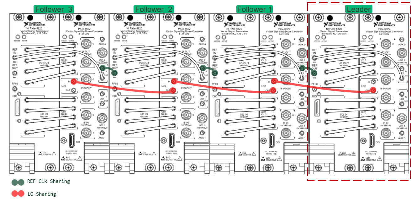
For a single chassis setup, follow the below steps to setup your phase coherent configuration:
  1. Insert your PXIe-5831 modules adjacently (side to side) in the chassis
  2. For the PXIe-5831 module setup, follow the steps described in the device getting started manual to configure the PXIe-5820 with the PXIe-3622
  3. Select your Leader device (typically the most right or the most left device)
  4. Using mmpx cables of matching length, connect the LO2 OUT of the Leader device to the LO2 IN of the adjacent device (Follower 1), and LO2 OUT of Follower 1 to LO2 IN of its adjacent device (Follower 2). Follow the same to share LO between all devices in your chassis
  5. Using mmpx cables of matching length, connect REF OUT of Leader to REF In of Follower 1, then REF OUT of Follower 1 to REF IN of Follower 2, etc...This will share the onboard Ref clock of the Leader with all the Followers. IF you would like to use PXI Reference clock as a reference, you can skip this step and you can configure it using the driver APIs as we will see in the Software section.
  6. The connections should look like this:
 

Software Configuration:

In the previous section, we discussed how we can synchronize the Leader device with the Following devices by sharing the LO and Reference Clock.  In this scenario, the Leader is programmed to distribute the trigger signal to all Followers in the system including itself. Two issues that arise here are trigger delay and skew. A trigger delay from the Leader to all the Followers and skew between each Follower device is inevitable, but this delay and skew can be measured and calibrated. To overcome this situation, NI-TClk synchronisation is used where its purpose is to have devices respond to triggers at the same time. The "same time" means on the same sample period and having very tight alignment of the sample clocks.
NI-TClk synchronization is accomplished by having each device generate a trigger clock (TClk) that is derived from the sample clock. Triggers are synchronized to a TClk pulse. A device that receives a trigger from an external source or generates it internally will send the signal to all devices, including itself, on a falling edge of TClk. All devices react to the trigger on the following rising edge of TClk.
NI-TClk has a set of APIs that can be called from LabVIEW to enable the homogeneous trigger alignment.

That being said, to configure a phase coherent multi-channel system, we need to set several properties for NI-RFSA and NI-RFSG such as the LO sharing and Reference clock, as well as enable the NI-Tclk trigger alignment between the devices.

For the PXIe-5830/1, there are few properties that need to be set in addition to those in a 5840/1 based system. For instance, you need first to set the selected ports for transmission and reception since the IF ports of the 5830/1 are bidirectional.
In addition, for the PXIe-5831 VST, you need to manually set the active LO channel you are targeting to configure since there are 2 LOs, LO1 used for the mmWave head connections and LO2 used for the IF path. In our case we will configure the LO2 channels.

Here is a summary of the steps required to configure RFSA/RFSG for Phase Coherent acquisition and Generation:


Configure Port:

To configure selected port with RFSA and RFSG, you need to place a driver specific property node.
For RFSA, navigate to Signal Path >> Advanced >> Selected Ports, possible values for IF mode are if0 or if1
For RFSG, navigate to Device Specific >> Vector Signal Transceiver >> Signal Path >> Selected Ports possible values for IF mode are if0 or if1


Configure Reference Clock:

To Set Reference clock, we mentioned several methods:
  • Leader shares its onboard reference clock with the Follower device, and each follower with its adjacent device in daisy chain mode. This means you need to set the Leader Reference Clock to Onboard and the Follower reference clocks to RefIn while enabling the reference clock export to RefOut terminal.
 
For RFSG, use the niRFSG Configure Ref Clock .vi to set the reference clock, and enable the reference clock export for the Leader and all Followers except the last one (since it is not sharing its signals with any other device),  using niRFSG property node by navigating to Clock >> Reference Clock Export Output Terminal


For RFSA, use the niRFSA Configure Ref Clock .vi to set the reference clock, and enable the reference clock export for the Leader and all Followers except the last one (since it is not sharing its signals with any other device),  using niRFSA property node by navigating to Clocking >> Ref Clock Exported Terminal


  • Leader and Followers are all synced to the PXI Reference Clock, assuming that the selected chassis provides an onboard OXCO clock source, for instance the PXIe-1095 has 2 options with and without onboard clock. Verify that your chassis provides access to a 10MHz reference clock before proceeding with this step.
 
For RFSG, use the niRFSG Configure Ref Clock VI with the PXI_CLK property as source for all devices:


For RFSA, use the niRFSA Configure Ref Clock VI with the PXI_CLK property as source for all devices:
 
  • Leader and Follower can all be synched to an external Reference Clock, in this case use the previous step with RefIn as a value for the clock reference source


Configure LO Sharing:

For the daisy chain setup, the Leader exports its onboard LO2 to the adjacent Follower device and each Follower with the next adjacent one.
With RFSA, using a niRFSA property node, you need to set in order, first the Active Channel with value= lo2,  followed by the LO Source (Signal Path >> LO Source) and the LO Export Enabled property (Signal Path >> LO Export Enabled) . The LO Export needs to be enabled for the Leader and all Follower devices sharing their LO (except the last one).
The LO Source on the Leader needs to be set to Onboard, unless you are using an external LO synthesizer such as the PXIe-5653, where you can set the source to LO_In.
For the devices receiving external LO, you need to set the LO frequency using niRFSA property SignalPath >> LO Fequency, where you read this value on the sharing device and you wire it to the receiving device.


Note - Setting LO Power: 

It is important to note that the accepted power for LO In is between 6 and 10dBm, so your external LO should follow this range, including the power output by LO2 from the Leader. The default power output from LO2 is around 5dBm, so you need to manually set the value of LO Out Power between 6 and 10 dBm before inputting the LO In Power to the Followers .
For niRFSA, You can access the LO power property from SignalPath >> LO Out Power
 
With RFSG, follow the same steps as with RFSA. Navigate to RF >> LO Out Enabled to export LO, RF>>LO Frequency (Hz) to read and write the LO frequency and  Device Specific >> Vector Signal Transceiver >> Signal Path >> LO Source to set the LO Source. 
To Set the LO Power property navigate to  Device Specific >> Vector Signal Transceiver >> Signal Path >> LO Out Power/LO In Power

Note - Using External Synthesizer:

If you are using the PXIe-5653 as a source to the Leader device, you need to connect its LO1 to LO2 port of the PXIe-5831 with 3dB attenuator, and set its LO1 to a supported value by the 5831. For this you can set your carrier frequency with the RFSG/RFSA driver then read the LO frequency property). Refer to below image for supported LO2 values with respect to the configured carrier:
 

Configure NI-TClk

To Configure NI TClk on generation and/or analyzer side, first you must obtain the session reference for each device including the Leader, then use TClk Synchronization APIs to configure the device for Homogeneous Triggers generation/analysis. Then enable TClk synchronization to align the triggers between the different devices and finally Initiate the generation/Acquisition where all devices start at the same trigger.
Note- This implementation of TClk is compatible with continuous acquisition/generation mode and does not support Start or Reference Trigger sharing.


Note - Synchronous Generation and Reception

The above cases synchronize multi-channel Tx paths or multi-channel Rx path. If you would like to synchronize the Tx and Rx paths together, then you need to consider the below modifications:
  • Share the LO between the Tx and Rx paths by setting the LO Source property in RFSA/RFSG to SG SA Shared on the Leader Device instead of Onboard while maintaining LO_In on the Followers. The SG SA shared property internally shares the LO between both paths as described in the Overview section. Setting the LO source to LO_In on the Followers ensures that both Tx and Rx paths use the same external reference LO
  • Include both RFSA and RFSG sessions in the list of devices wired to niTClkConfigure for Homogeneous Triggers VI. This ensures that the trigger alignment happens on all devices to initiate both generation and acquisition at the same trigger

Following the above physical and Software configurations will ensure a phase coherent multi-channel generation and /or analysis. You can calculate the channel to channel phase and amplitude skew with respect to the Reference device for both Tx and Rx paths.
To test this, first you need to equalize the skew on the analysis side where you can generate a CW tone signal from the Leader Tx channel or any external generator then wire it with a splitter to all Rx channels with matching cables. Then you can measure the channel to channel skew as well as the mean difference between the channels. The mean difference (phase and amplitude) can then be equalized to have a similar behavior between the Folllowers compared to the Leader, so the mean can be brought to 0 +/- skew calculated which is a benchmark of the stability/accuracy of the multi-channel system including the cabling and external signal conditionning components used.

After this step, you can then calculate the skew on the generation side using the equalized Rx channels of the same system. For this step, all you need to do is connect the Tx/Rx channels in loopback on each VST (you can also consider cross connections where Tx is connected to Rx of adjacent device and vice versa) then you run your synchronized code on generation and you calculate the skew on receiving side similar to the previous step.

You can test the setup described in this article by downloading an example code posted on NI Community called Multi-Channel Phase Coherent Generation & Acquisition with PXIe-5830/1 IF only.

Next Steps

The steps described in this document are the foundations of multi-channel phase coherent system. You can then generate complex scenarios and stream them to the VST for generation to stimulate your device under test (DUT) such as multi-channel TRM or beamformer, then use the phase coherent acquisition to capture the DUT response and analyze it onboard on the FPGA or stream it to RAID for offline analysis.

Certain applications i.e. measuring antenna array elements coupling, require not only phase coherent acquisition and generation but also phase alignment between all channels including the Leader Device. Such applications require certain level of System Level Calibration to compensate for irregulaties introduced by external components, impedance mismatch, cabling, etc... And also require Flatness correction and compensation for phase linearity errors on the Leader device, so not only we mimic the behavior of the Leader on the Followers but also we correct the behavior of the Leader with respect to the specific signal parameters to be used such as central frequency, bandwidth and power levels.