Prerequisites
This tutorial assumes completion of HDL Coder exports imported per HDL Coder and LabVIEW FPGA: Importing HDL Coder Exports in LabVIEW FPGA .
Make sure the following software versions are installed.
Creating a Host VI for the LabVIEW FPGA VI
In order to simulate a LabVIEW FPGA VI with DMA FIFOs and other host communication methods, NI recommends creating a host VI. This host VI can be a testbench, or it can be closer to the final design which will interact with the FPGA design. For this tutorial, a testbench approach will be used to demonstrate the functionality of the imported IP.
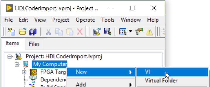
- In the LabVIEW project, right-click My Computer and select New >> VI to create a new VI in the host PC context.
- On the front panel of the VI, right-click to open the Controls Palette. Select Graph >> Waveform Graph.
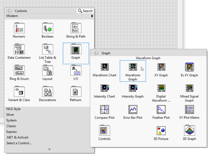
- Click on the front panel to place the Waveform Graph. Add two more Waveform Graphs by following the same steps.
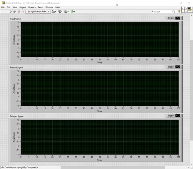
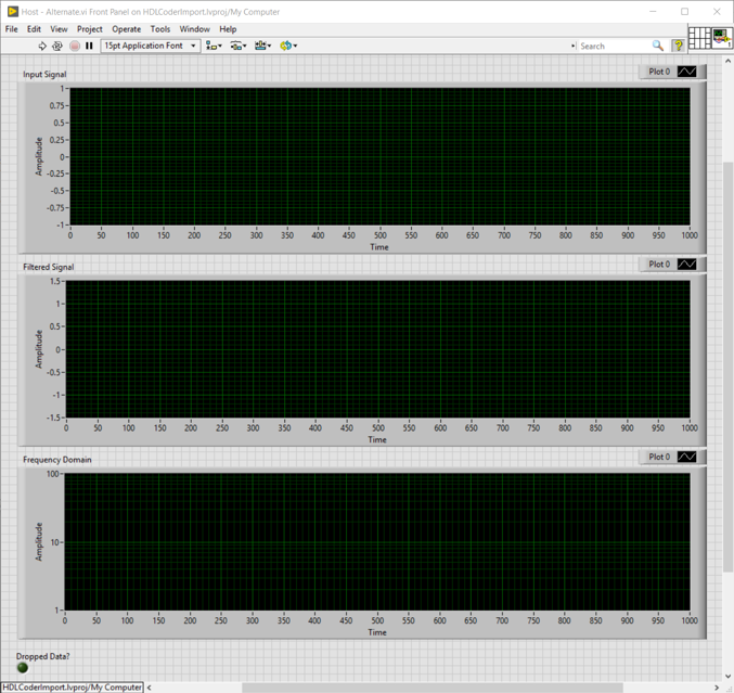
- Resize and label the Waveform Graphs as shown below.
- Save the VI.
- Switch to the block diagram by pressing Ctrl + E or selecting Window >> Show Block diagram.
- Create the code to generate an input signal:
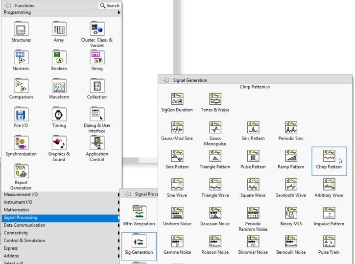
a. Right-click the block diagram to open the Functions Palette, then select Signal Processing >> Signal Generation >> Chirp Pattern. Place the Chirp Pattern VI on the block diagram.
b. Wire the Chirp Pattern VI as shown below.
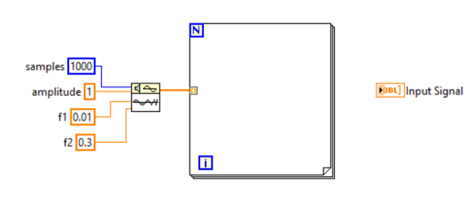
c. From the Functions Palette, select Numeric >> Conversion >> To Fixed-Point. Place this fucntion in the For Loop.
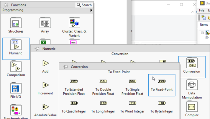
d. From the Functions Palette, select Numeric >> Numeric Constant to drop a Numeric Constant on the block diagram.
e. Right-click the Numeric Constant and select Properties. Configure the Data Type to a fixed-point representation that matches the DMA FIFOs configured in [Part 2] HDL Coder and LabVIEW FPGA: Importing HDL Coder Exports in LabVIEW FPGA.
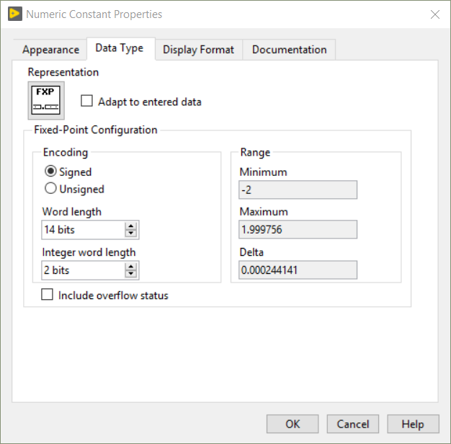
f. Click OK.
g. Wire the Input Signal as shown below.
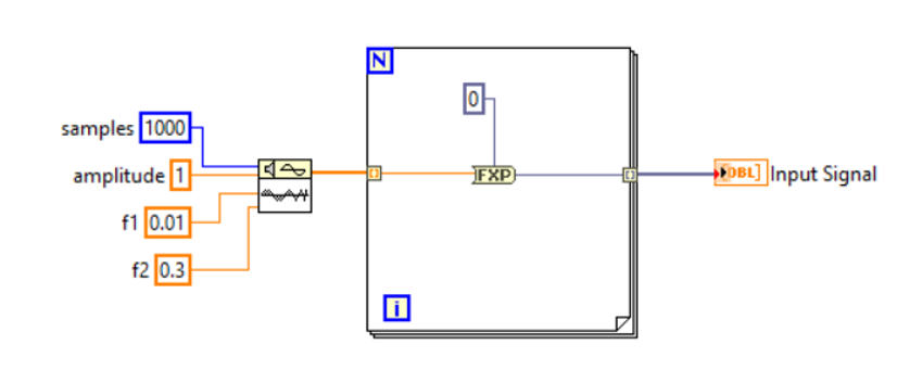
- Create code to communicate with the FPGA VI. The functions used in this section are all located in the Functions Palette under FPGA Interface.

a. Drop an
Open FPGA VI Reference and double-click the node to open the
Configure FPGA VI Reference window.
b. Select VI and then navigate to the FPGA VI created in [Part 2] HDL Coder and LabVIEW FPGA: Importing HDL Coder Exports in LabVIEW FPGA, then click OK. This will configure the Open FPGA VI Reference to refer to the FPGA design you created in the previous part.

c. Click OK.
d. From the FPGA Interface palette, drop an Invoke Method node.
e. Wire the FPGA VI Reference Out and error out outputs of the Open FPGA VI Reference node to the corresponding inputs of the Invoke Method.
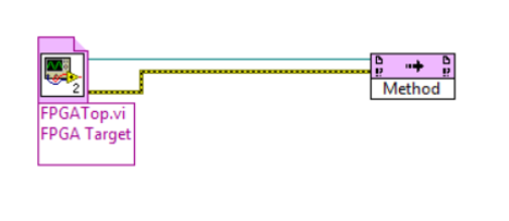
f. Click on the Method text on the Invoke Method and select the Write method for the Host to Target DMA FIFO.
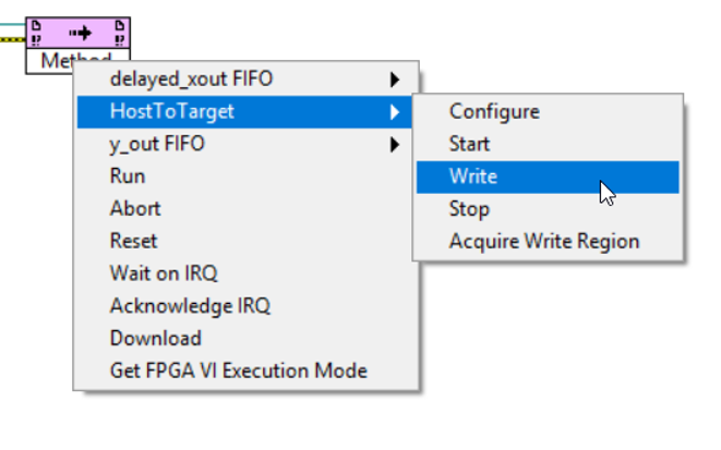
g. Select the Read method for each of the Target to Host DMA FIFOs by repeating steps d through f.
h. Place a Read/Write Control node. Wire the FPGA VI Reference Out and error out outputs from the previous node to the inputs of the new Read/Write Control node.
i. Click on the node and select the Dropped Data? Boolean control from the FPGA VI.
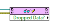
j. Place a Close FPGA VI Reference node and wire the FPGA VI Reference Out and error out outputs from the Read/Write Control node to the Close FPGA VI Reference node’s corresponding inputs.
- Finish wiring the remaining inputs and outputs of the VI as shown below. If desired, add a Simple Error Handler VI and an indicator for the Boolean Dropped Data?
Note: If the design is encountering dropped data, consider reducing the size of the waveform being processed or increasing the size of the DMA FIFO buffers. For more information on DMA buffer sizes, refer to Avoiding Buffer Errors in DMA Applications .

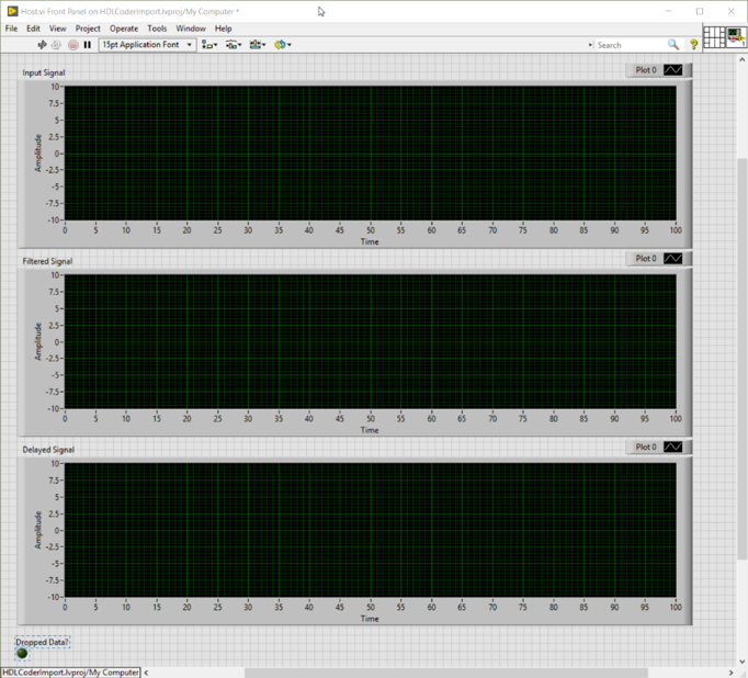
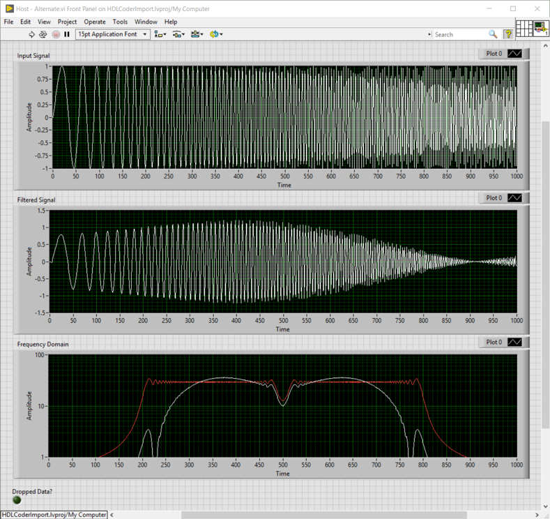
- Alternatively, match the MATLAB test bench output for the FIR filter by modifying the VI as shown below. Note the use of the FFT.vi, Absolute Value, Build Array, and the modifications to the third graph which is now configured for logarithmic scaling.

- Save the VI and LabVIEW project.
Simulating the FPGA VI
Simulation allows debugging and further troubleshooting of the FPGA VI before embarking on the potentially lengthy FPGA compilation process. Debugging at this stage can highlight problems and allow improvements to the code design before moving to a real-world hardware implementation. FPGA VIs in simulation mode allow the use of probes, breakpoints, and other typical LabVIEW debugging tools as well as tools unique to FPGA such as sampling probes.
Note that one of the advantages of using the IP Integration Node as opposed to Component-Level IP is that the IP Integration Node supports native LabVIEW FPGA simulation. To simulate Component-Level IP, a third-party simulation tool is needed. For more information on FPGA simulation, refer to Testing and Debugging LabVIEW FPGA Code and the LabVIEW FPGA Module Help.
Complete the following steps to simulate the design created in this tutorial:
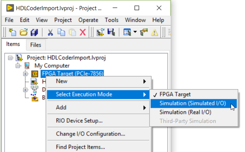
- In the LabVIEW project, right-click the FPGA Target and select Select Execution Mode >> Simulation (Simulated I/O) to configure LabVIEW to run the FPGA code in simulation.
- Open the host VI and click the Run arrow to run the VI.
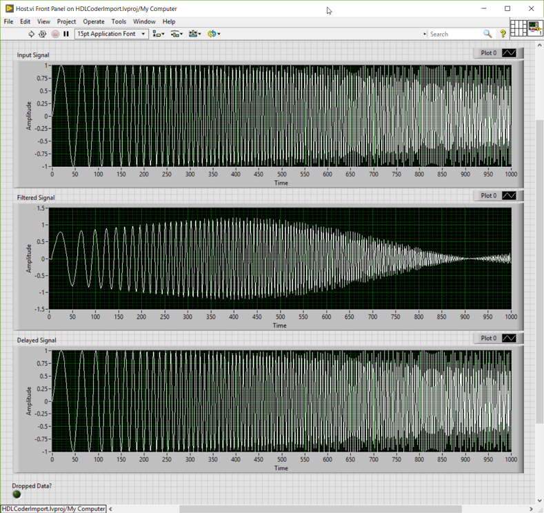
- Note that the output correctly updates to show the filtered signal, and that the delayed output and input match. If you use the alternate host VI design to match the MATLAB test bench output, note that the Frequency Domain graph should look similar to the test bench outputs.
Compiling and Running the FPGA VI
At this point, the FPGA code can be compiled as with any other LabVIEW FPGA code. Note that the execution mode for the FPGA target in the project must be set to FPGA Target instead of Simulation (Simulated I/O) in order to compile the code into a bitfile. Once the bitfile is generated, you can deploy the FPGA code on the FPGA hardware. For more information about compiling FPGA code and deploying LabVIEW FPGA bitfiles, refer to Compiling, Downloading, and Running FPGA VIs in the LabVIEW FPGA Module Help.