Introduction
Taking a hands-on approach to learning digital logic can be difficult without the need for students to learn complex hardware descriptive languages. Multisim’s Programmable Logic Device (PLD) schematic, along with support for leading Digilent teaching hardware allows students to put the fundamentals of digital theory into practice. The PLD schematic allows educators and students to create graphical logic diagrams like those found in textbooks and deploy these to educational FPGA boards such as the Digital System Development Board (DSDB).
Timing is a critical part of digital design. Because of the inability of software-based simulations to meet the speed of hardware, gaining an understanding of timing can be difficult.
This tutorial provides an example of how you can develop counters using the DSDB or any other Digilent FPGA board and use these to control the onboard 7-segment displays using Multisim and the PLD schematic.
For more details on installing and setting up the DSDB in Multisim, refer to the Getting Started with Digilent Boards in Multisim guide.
Setup Requirements
You will need the following for this tutorial:
- Multisim 14.0.1 or higher, Education Edition.
- National Instruments Digital Systems Development Board.
- Xilinx Vivado 2014.x or 2015.x
Or
LabVIEW 2015 SP1 FPGA Module Xilinx Tools Vivado 2014.4.
- If you use this option,
an additional executable must be run. This can be found in
- <NIFPGA install dir>/programs/Vivado2014_4/data/xicom/cable_drivers/<nt or
- nt64>/digilent/install_digilent.exe.
Refer to Multisim Won't Recognize My Digilent FPGA Board for more information.
Simulation Schematic
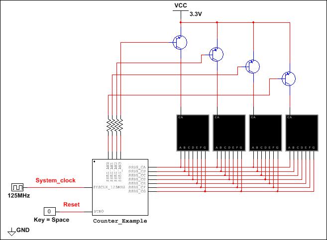
The top level schematic, as part of this project, allows for simulation. It places the PLD logic in place around the IO contained on the board. To achieve this we use a PLD sub-circuit. The PLD sub-circuit allows us to place the PLD code within a single component as if it was being run on the FPGA.
Create a subcircuit that represents the PLD on the DSDB
- Open a new blank design.
- Select Place»New PLD subcircuit.
- Select NI Digital Systems Development Board from the drop-down menu and click Next.
- Enter Counter_Example for the PLD subcircuit name and click Next.
- Select the connectors that you will be using on the DSDB board. For this tutorial, select:
- SYSCLK_125MHZ – 125 MHz clock on the DSDB board.
- BTNO – Push button located on the DSDB board to reset the counter.
- SSEG_AN0 – SSEG_AN3 – Four digital lines to control which of the four 7-segment displays to display.
- SSEG_CA – SSEG_CG – Seven digital lines to control the segments in the 7-segment displays.
- Click Finish and click again to place the PLD subcircuit on the design.
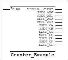
- Right-click on the symbol and select Edit symbol/title block to launch the Symbol Editor.
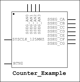
- Edit the symbol as shown below:
- Save the symbol and close the Symbol Editor.
The changes are reflected on the schematic.
Add the other DSDB components
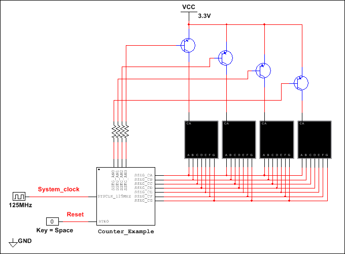
- Place and wire the following components:
- DIGITAL_CLOCK – Set to 125 MHz. This represents the 125 MHz clock on the DSDB.
- Digital Ground.
- Interactive Digital Constant – This represents the push-button on the DSDB that will be used to reset the counter.
- Four 100 Ω resistors.
- Four 2N2904 PNP transistors – These represent the transistors on the DSDB that drive the 7-segment displays.
- Four SEVEN_SEG_COM_A 7-segment displays.
PLD Schematic
This section details how to create the digital logic within the PLD schematic.
In this example we are creating a simple up-counter and the required logic to control the four 7-segment displays. The PLD code must control the illumination of the 7-segment displays and perform the up-counter operation.
- Double-click the PLD subcircuit and select Open subsheet from the Hierarchical Block/Subcircuit window that appears.
- Complete the contents of the PLD subcircuit as shown below.
Note: You can skip this step and use the completed files that are referenced at the end of this document for the remainder of this tutorial, but it is recommended that you read the descriptions of the PLD subcircuit functionality below.
The figures below show the three main sections of the PLD schematic.
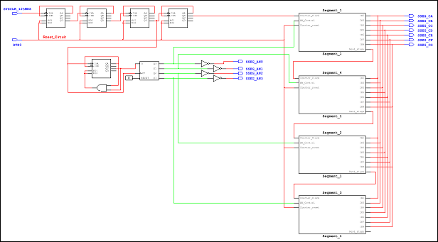
The Main Counter provides a clock signal to both the update counter and the display counter:

The Update Counter selects the 7-segment display to be updated:

The Display Counter determines the value to be updated on the selected 7-segment display:
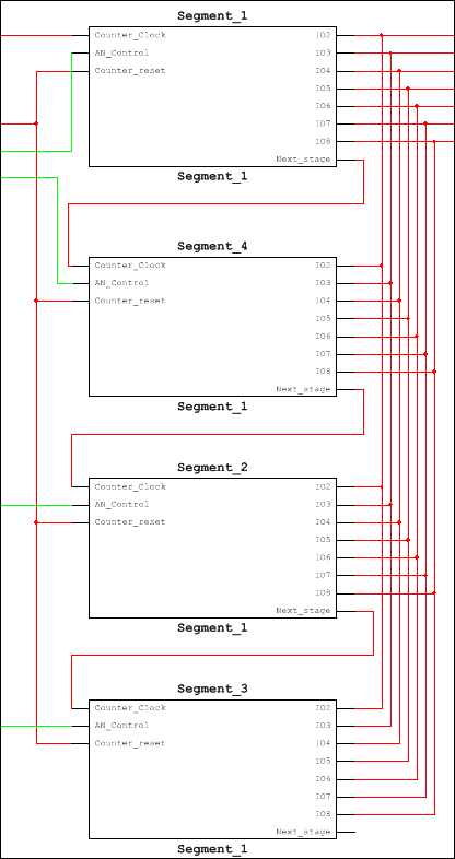
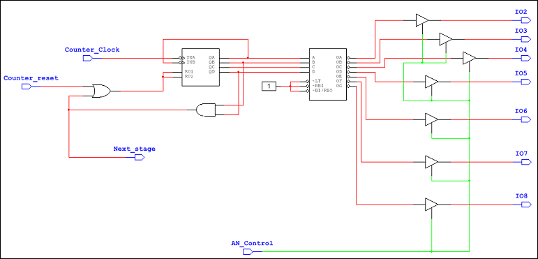
Each of the four display counter blocks are represented by a subsheet containing:
- A counter that calculates the value for that display before passing that value onto the next display counter block.
- A 7-segment decoder to take the counter value and output it to the display.
- A buffer for each of the seven lines leading to the display.
Simulating and Deploying Logic
The above PLD code can be simulated by running the top level circuit and viewing the display on the virtual 7-segment displays. During simulation, the displays are illuminated one at a time to show the count.
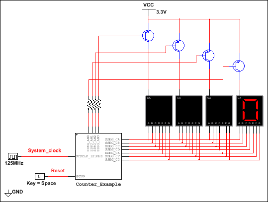
Within the simulated PLD code a shift register in the update counter section controls which of the
7-segment displays is updated. This is then passed out of the PLD schematic and the transistors regulate which of the displays gets illuminated. The virtual BTN0 button can be triggered to reset the counter using the space bar.
Exporting to the PLD board
In this step, you will deploy the PLD code to the DSDB board, where the components on the top-level schematic are replaced with physical components.
Because the hardware operates much quicker than the simulation, some modifications must be made to make the 7-segment displays on the DSDB readable, as opposed to appearing constantly lit. This can be done by adding additional counters to step-down the clock frequency, as shown below:

Rather than modifying your existing simulation schematic, you can open DSDB for board.ms14, and export its contents to the DSDB. This file contains only the components from the PLD subcircuit in DSDB for simulation.ms14.
- Open DSDB for board.ms14 in Multisim.
- Select Transfer»Export to PLD.
- Step 1 of the PLD Export dialog box displays.
- Select Program the connected PLD and click Next to display step 2.
- Select Xilinx Vivado Design Suite 2015.4 64-bit from Select a tool to use.
The actual selection will depend on your OS/installation setup. - Click Refresh to detect the attached DSDB.
- Click Finish.
The PLD logic is exported to the DSDB. This may take several minutes. When complete, the
7-segment displays will start counting.
To reset the count, press switch BTN0.