Differentiate Previous Generation R Series with Current Generation R Series
There are two main aspects that can be used to distinguish between previous generation R Series and newer generation R Series:
- Communication Interface: All previous generation R Series have a PCI or PXI interface. Current generation R Series have USB or PCIe or PXIe.
- FPGA Model: Newer generation R Series are equipped with a high-performance Kintex-7 FPGA while older R Series use a Virtex-5 FPGA.
For more details on each R Series model you can go to the following link and consult the table 1. NI R Series Multifunction RIO Frequently Asked Questions (FAQ)
Using the Fixed-Point Data Type With R Series Devices
By default, FPGA I/O Nodes for analog input and output channels on USB/PXIe/PCIe R Series devices use the fixed-point data type, which provides data in calibrated engineering units. For FPGA applications, the fixed-point data type is advantageous over floating point because it can be processed much faster and can significantly reduce the number of resources you use on the FPGA. For a more detailed discussion on the fixed-point data type, see LabVIEW FPGA Floating-Point Data Type Support. NI recommends using the fixed-point data type for most FPGA applications.
There are, however, cases where using raw data over calibrated data is advantageous such as when streaming data to achieve the maximum acquisition rate (1 MS/sec) on all AI channels simultaneously. Additionally, raw data uses the I16 data type, which allows you to join it with other I16's to create a single I32 or I64 that can be placed in a single DMA FIFO element for the most efficient transfer to the host. Another case where raw data is advantageous is when FPGA resources are limited and the additional processing required for fixed-point data exhausts all the available FPGA resources.
Changing FPGA I/O Configuration From the LabVIEW Project Explorer
Once you’ve identified calibrated or raw as your preferred data type, you may need to change the I/O configuration. For USB/PXIe/PCIe R Series devices, calibrated is the default so these steps may not be necessary.
-
From the LabVIEW Project Explorer right-click FPGA Target»Change I/O Configuration… as shown in Figure 1.
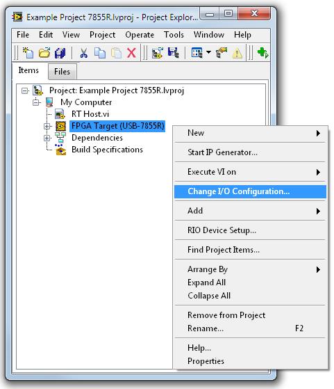
Figure 1. Change the R Series I/O configuration from the LabVIEW Project Explorer
- In the Configure R Series I/O dialog box (Figure 2):
- Select applicable AI Terminal Mode
- Change the AI/AO Data Type to Calibrated or Raw.
- Select the desired voltage range.
- If desired, you can adjust the voltage range per channel by selecting the applicable channel(s) and then changing the Voltage Range.
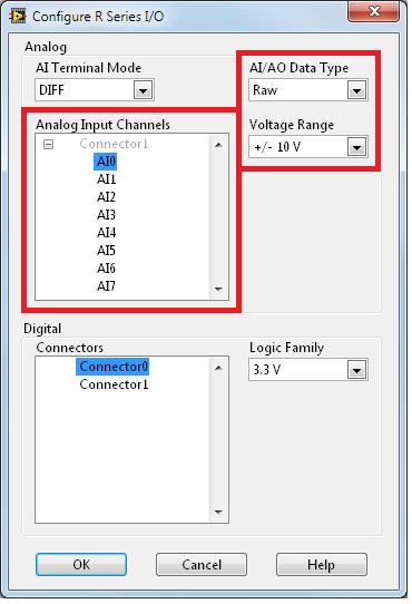
Figure 2. Configure R Series I/O
-
After you have configured the I/O and placed an FPGA I/O Node on the block diagram, the calibrated data node appears as shown in Figure 3.
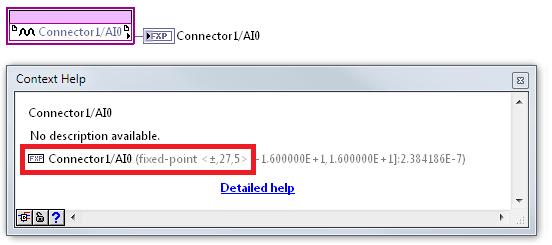
Figure 3. Appearance of FPGA I/O Node—Calibrated (Fixed-Point) Data Type
-
An FPGA I/O Node for raw data appears as shown in Figure 4.
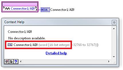
Figure 4. Appearance of FPGA I/O Node—Raw (I16) Data Type
Migrating Code From Previous-Generation R Series to Current-Generation R Series Devices
LabVIEW FPGA code written for previous generations of R Series devices should run without error on USB/PXIe/PCIe R Series devices. However, after converting binary data to engineering units, you may notice that your current-generation R Series device yields a different result than that obtained by a previous-generation R Series device. This is because of a difference in the way calibration is implemented.
On previous-generation R Series devices, raw data from the analog-to-digital converter (ADC) is calibrated in hardware and passed to LabVIEW where it is read as an I16 with an FPGA I/O Node. This is slightly different for USB/PXIe/PCIe R Series devices where uncalibrated raw data is passed directly to LabVIEW from the ADC. From there, the data then needs to be calibrated in software. This difference in calibration is mostly responsible for inconsistencies you may see between devices.
The device’s operating voltage range also contributes to a difference in measurements obtained from different devices. You can find this range in the applicable R Series Specifications manual. For example, a previous-generation R Series device has a slightly smaller operating voltage range (±10 V) than USB/PXIe/PCIe R Series devices (±10.63 V). This difference changes the weight of each least significant bit (LSB), which prevents a 1-to-1 mapping of binary to nominal values between targets. As such, you must be aware of these subtle differences and account for them when developing code intended for use with multiple R Series devices.
Calibrating Raw Data for USB/PXIe/PCIe R Series Devices
When a USB/PXIe/PCIe R Series analog channel is configured for raw data and read into LabVIEW through an FPGA I/O Node, the resulting binary (I16) data is uncalibrated. You can calibrate this data through the following process, which requires a LabVIEW host VI (Windows or Real Time) and the binary to nominal VI (analog input) or nominal to binary VI (analog output). These VIs are accessible from NI USB/PXIe/PCIe R Series examples.
From your FPGA VI (Figure 5):
- Analog Input
- Acquire the measurement using an FPGA I/O Node and wire the output to an indicator.
- Using an FPGA I/O Property Node, select the LSB Weight and Offset properties for the analog input voltage range you desire.
- Bundle the properties into a cluster and wire the cluster to an indicator.
- Analog Output
- Create an FPGA I/O Node for an analog output channel.
- Create a control and wire it to the input of the FPGA I/O Node.
- Create an FPGA I/O Property Node for your analog output channel (right-click, Select Item»FPGA Target) and select the LSB Weight and Offset properties.
- Bundle the properties into a cluster and wire the cluster to an indicator.
- Save and compile the VI.
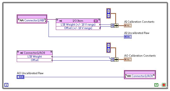
Figure 5. Extract calibration data for analog input on USB R Series using an FPGA I/O Property Node and write analog out.
From your host VI (Figure 6):
- Open a reference to the FPGA VI created in the previous section using the Open FPGA VI Reference VI.
- Configure the Open FPGA VI Reference to run the FPGA code written to acquire the calibration coefficients.
- Use a Read/Write Control to obtain the AI Calibration Constants cluster, AI1 Uncalibrated RAW value, and AO Calibration Constants cluster.
- Wire the AI Calibration Constants output of the Read/Write Control to Binary to Nominal.vi. The VI can be found at C:\Program Files (x86)\National Instruments\LabVIEW 20XX\examples\R Series\Device Specific\PXIe MIO Devices\Stream Data\subVIs
- Create a constant on the target input to Binary to Nominal.vi and select the applicable R Series device.
- Wire the outputs of Binary to Nominal.vi to indicators and display the results.
- Create a control to set the desired analog out value and wire it to Nominal to Binary.vi.
- Wire the AO Calibration Constants output of the Read/Write Control to Nominal to Binary.vi.
- Add a second Read/Write Control node and select the analog out channel from the FPGA VI.
- Wire the output of Nominal to Binary.vi to the AO Uncalibrated Raw input of the Read/Write Control.
- Encapsulate the code in a While Loop.
- Close your FPGA VI reference using the Close FPGA VI Reference VI.
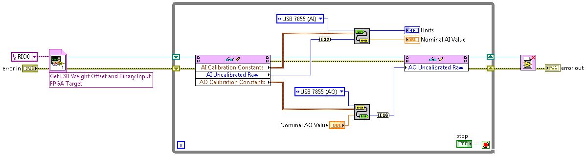
Figure 6. Host VI Used to Calibrate Raw Data Acquired With an FPGA