Solution
Presented below are two of the many methods used to de-bounce a mechanical switch
SR Flip-Flop De-bouncerYou can use a latch or an SR flip-flop to eliminate signal bounce or noise caused by the switching of a mechanical device (switches, buttons etc.). When the switch occurs, only one input is affected immediately before stabilizing. This is followed by the second input bouncing before the contact stabilizes. Both inputs are never bouncing at the same time so the output of the latch will never change due to signal bounce. Directly below is a schematic for a latch de-bouncing circuit.
RC Circuit De-bouncer
Another approach to debouncing uses a Resistor (R) and Capacitor (C) circuit to remove bounce at the input of a Schmitt Trigger or other high input impedance logic element (a CMOS inverter is shown). The Schmitt Trigger output provides the de-bounced signal to the rest of the circuit. The figure below contains the schematic for an RC de-bouncing circuit.
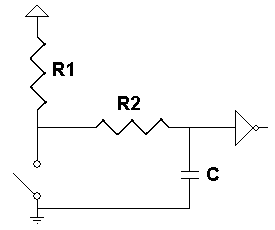
When the switch is flipped from open to closed, C dissipates its charge to ground through R2. The equation for the voltage across the capacitor (VC) as a function of time (t) while it is discharging is given by Equation 1.
VC(t) = VDC (exp(-t / R2C)) (Equation 1)
This period is the transition from logic high to logic low. We would like this transition to take longer than the total bounce time seen on the system. An easy way to do this is to let VC = logic low for the Schmitt trigger, pick a standard or available value for C, and measure the bounce time of the system using a oscilloscope or logic analyzer. The equation for R2 is then given by Equation 2.
R2 = -t / C * ln (Logic_Low / VDC) ] (Equation 2)
When the switch is flipped from closed to open, C charges to VDC through the series combination of R1 + R2. The equation for VC(t) while it is charging is given by Equation 3.
VC(t) = VDC ( 1 - exp(-t / (R1 + R2)C )) (Equation 3)
This period is the transition from logic low to logic high. We would like this transition to take longer than the total bounce time seen on the system. Using the same value for t as before, and the value of R2 found using Equation 2, the equation for R1 is given by Equation 4.
R1 = { -t / [C * ln (Logic_High / VDC)] } - R2 (Equation 4)
Example: My mechanical switch is causing 10 micro seconds of bounce at my PCI-6510 CMOS input. I have +5V DC available for external circuitry and I have a 10 nano Farad capacitor available. I want to build an RC de-bouncing circuit.
- Solve for R2 using Equation 2. t = 10 us, C = 10 nF, Logic_Low = 1.3 V, VDC = 5 V. R2 = 742 Ohms.
- Solve for R1 using Equation 4. t = 10 us, C = 10 nF, Logic_High = 3.7 V, VDC = 5 V. R1 = 2579 Ohms.
- Use a non-inverting CMOS line buffer in between the mechanical switch and the PCI-6510's input line.