Solution
To prevent this issue, use one of the methods described below.
Method 1: Use a Spare Intermediate TerminalIf the external signal is not generated synchronously to the synchronization clock used by the Timing and Synchronization module, there is no way to guarantee that the signal will be stable within the setup-and-hold window. Therefore, the first method involves synchronously routing the external trigger first from the source terminal to a single spare intermediate terminal. This makes the intermediate signal only change at deterministic times (i.e. when an edge of the synchronization clock occurs). Then create synchronous routes from this intermediate terminal to your desired destination terminals. For example, in the case mentioned above where you want to route an external trigger on
PFI0 to multiple
PXI_Star lines, you could create the following synchronous routes:
- PFI0 to any single available PXI_Trig line (e.g. PXI_Trig0).
- From the PXI trigger line chosen in step 1 to the various destination PXI Star lines.
You can make these routes using the
niSync Connect Trigger Terminals VI or by using the
Routing tab of the MAX Test Panel for the module.
Notice that in order for this method to resolve the issue, the signal must be able to travel between the intermediate terminal and the destination terminals in less than one synchronization clock cycle. For an example calculation, consider implementing the case above where you are routing a trigger from a PXI Trig line to several PXI Star lines on a PXIe-6674T. The PXIe-6674T has a typical delay of 19.4 ns from the
PXI_Trig to
PXI_Star lines. This means that your synchronization clock would have to be <~51 MHz in order for this workaround to work properly.
Have in mind that using this method will increase the overall route delay by one clock cycle.
Method 2: Make the Trigger Input SynchronousThe second option is to ensure the external trigger meets the setup and hold timing to begin with. This is done by synchronously generating the trigger externally before connecting it to the input terminal of your Timing and Synchronization module.
In order to do this, you will need to share your chassis’
PXI_Clk10 with an external device that can generate a trigger synchronous to this clock. The device must be able to output the trigger fast enough to meet the setup and hold requirements at the PFI input. Since the input trigger now meets the timing requirements, the signal can be synchronously routed to several destinations, such as
PXI_Star lines, without the need for an intermediate terminal as required in Method 1.
To implement this method, complete the steps below:
- Make the following connections for your hardware:
- Cable ClkOut on your Timing and Synchronization module to a clock input of your external hardware
- Cable the trigger output of your external hardware to a PFI line on the timing module
- In software, configure the following routes:
- Route PXI_Clk10 to the ClkOut terminal of your timing module. You can make this route using the niSync Connect Clock Terminals VI or by using the Routing tab of the MAX Test Panel for the module.
- Create synchronous route(s) from the PFI line you have cabled to the PXI_Star line(s) you want to use. You can make these routes by using the niSync Connect Trigger Terminals VI or by using the Routing tab of the MAX Test Panel for the module.
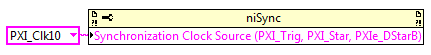
- Set the Synchronization Clock for the PFI lines to be PXI_Clk10. You can do this in the Routing tab of the MAX Test Panel or with an niSync Property Node by selecting Synchronization Clock Properties>>Synchronization Clock Source (PXI_Trig, PXI_Star, PXIe_DStarB). Set this property to PXI_Clk10, as shown below:
Notice that in order for this method to resolve the issue, the generated trigger will need to reach the
PFI line within a clock cycle of
PXI_Clk10 and meet the setup and hold time of the timing module. To determine if your setup is capable of meeting this timing requirement, you can make the following calculations:
Note: if the calculations seem unclear, please refer to the example at the end of this section for further clarification.
- Determine the trigger Setup Time required by your timing module. This can be found in your timing module's specifications.
- If the setup time determined in Step 1 is with respect to ClkOut, skip this step. Otherwise, add the PXI_Clk10 to ClkOut Delay to the Setup Time. This can be found in your timing module's specifications.
- Subtract the value calculated in steps 1 and 2 from 100 ns, which is the period of the 10 MHz clock.
- The resulting value is the time remaining for the following tasks:
- Routing PXI_Clk10 to your external hardware
- Generating a trigger in the external hardware
- Routing the generated trigger back to a PFI line of the timing module
The following timing diagram illustrates the delays between the clock's arrival at various terminals in your setup.
Tco represents the time calculated in step 4 above.
For an example calculation, consider the PXIe-6674T. This module has a
Setup Time of 13.2 ns specified with respect to
PXI_Clk10. So we need to also add the
PXI_Clk10 to ClkOut Delay to this value. The maximum delay is specified as 47.75 ns. Therefore, the setup requirement with respect to
ClkOut is 60.95 ns (13.2 ns + 47.75 ns).
Since the period of the synchronization clock is 100 ns, we can subtract this value to find the time left to route the clock from
ClkOut to our external hardware, generate the trigger, and route that trigger to our
PFI line. In this example, we are left with 39.05 ns for these tasks.
Now let’s say we’re using 1 m cables to connect
ClkOut to the external device's clock input and to connect the device's trigger output to the
PFI input (so 2 m total). Typical propagation delay through a cable is ~5 ns/m, so this would use up ~10 ns (5 ns/m * 2 m) of the external timing budget, leaving us with 29.05 ns for the external device itself to receive the clock and generate the trigger (this timing parameter is typically called "clock-to-output" time). Therefore, you must ensure that the external device's clock-to-output time is 29.05 ns or less.
Hold timing must also be analyzed. In this example, the hold time requirement for
PFI inputs for the PXIe-6674T is 1.1 ns. Hold timing is easily achieved in this example, because the typical delay of the clock from
PXI_Clk10 to
ClkOut (20.2 ns) is substantially more than the hold requirements of 1.1 ns. So we're guaranteed that the signal at the
PFI input will not change within 1.1 ns of the
PXI_Clk10 edge occurring.