Solution
It is true that the FPGA on-board clock on your target is running at 40 MHz. While loops running on the FPGA will use the top-level clock, which defaults to the on-board clock. Different function nodes you add to the block diagram will take a different amount of ticks to execute, where an empty while loop would take two ticks by itself. In principle, you would need to sum up all tick contributions in the while loop to get the total amount of ticks in the longest combinatorial path in order to calculate the overall loop rate.
For example, summing up two numbers would count up to 5 ticks (see figure below): One for the x control, one for the addition node, one for the x+y indicator and two for the while loop itself:
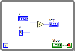
This would then be able to run at 40/5 = 8 MHz.
Same principle goes for reading or writing to a digital FPGA I/O Node which also takes one tick to execute:
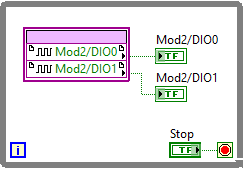
The loop above takes 4 ticks to execute and would thereby run at 10 MHz. The bottleneck might in this case be the digital module itself. Using a module such at the NI 9201 with an update rate of 100 ns, both code and module would set the limit to 10 MHz. However, a module such as NI 9381 with an update rate of 1 µs would limit the sample rate to 1 MHz.
Due to the fact that the code in both figures above consists of few components that all need one tick each to execute, you would normally replace the while loop with a SCTL (Single-Cycle Timed Loop). This would allow you to run each of the code examples at 40 MHz (i.e. run the full combinatorial path within a single clock tick).
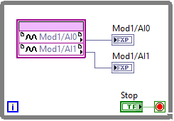
However, nodes that require more than one tick to execute cannot be used in a SCTL, but must be used in a while/for loop for repeated execution. One such example is the analog FPGA I/O Node, which normally requires over a hundred ticks to execute. Assuming that a benchmark test has shown that the node would need 140 ticks to execute, the following code requires 143 ticks and thus executes at roughly 280 kHz:
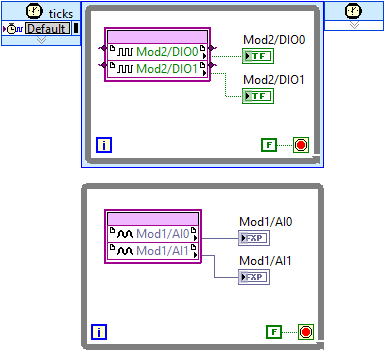
Thus, if digital and analog I/O are placed in the same loop, the analog FPGA I/O Node would be the limiting factor to the overall loop rate.
The solution, not to limit the digital reading and writing, would be to separate the analog and digital nodes to different loops, for example a SCTL for the digital I/O and a more slowly running while loop for the analog I/O: