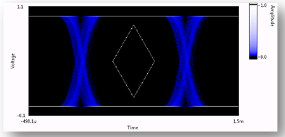
The blank area on the eye diagram becomes smaller due to noise and jitter. As shown in Figure 4, on the basis of removing jitter and noise, the distance of the blank area on the eye digram on the horizontal axis is called Eye Width. When the data superimposed on the eye diagram is sufficient, the eye width is well reflected. The stability time of the signal on the transmission line; similarly, the distance on the vertical axis of the blank area on the eye diagram is called Eye Height. When the data superimposed on the eye diagram is sufficient, the eye height reflects the transmission line very well. The noise margin of the upper signal. At the same time, the highest eye height in the eye diagram is the best judgement moment.

Figure 4: Eye Height and Eye Width
Before and after sampling, the digital signal needs to have a certain setup time and hold time. The digital signal should be stable during this period to ensure correct sampling, as shown in the blue part of Figure 5.1. For the input level decision, the high level voltage value is required to be higher than the input high level VIH, and the low level voltage value is input with the low level VIL, as shown in the green portion of Figure 5.1. Therefore, we can know that the earliest sampling time and the latest sampling time are shown in Figures 5.1 and 5.2.
Figure 5.1: Sampling and judgement a

Figure 5.2: Sampling and judgement b
At the optimal sampling time, the bit error rate of the sample is the lowest, and the bit error rate increases as the sampling time moves to both sides of the time axis, as shown in Figure 6. Therefore, the engineering often also draws a curve of the bit error rate during the signal sampling period, called the Bathtub Curve.

Figure 6: Bathtub Curve
In the actual test, in order to improve the efficiency of the testing, the method often used is Mask Testing. That is, according to the requirements of signal transmission, an area (such as the diamond-shaped area in Figure 7) is specified on the eye diagram, and all the left and right signals are required to appear outside the area. Once a signal appears in the diamond area, the test fails.

Figure 7: Mask Testing
3 Tools from NI
For transmission performance test analysis of digital signals, acquisition and analysis can be separated.
At the acquisition end, it is necessary to select an oscilloscope with the appropriate sampling rate, appropriate bandwidth and effective quantized bits according to the actual signal frequency, bandwidth, level characteristics, etc. NI provides a variety of oscilloscope cards for measurement, among them, PXIe-5186 oscilloscope can achieve 12.5 GS/s sampling, 5GHz bandwidth.
On the analysis side, you cna use the Signal Processing Toolkit (Function Palette - Signal Processing) in LabVIEW to perform simple processing on digital signals, including waveform measurement, analysis, and transformation. Testing for high speed digital signals;
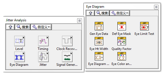
LabVIEW also includes the Jitter Analysis Toolkit VIs, which offer VIs for clock recovery, eye diagram measurements, jitter measurements, level detection, jitter signal generation, and timing measurements.
The correlation display analysis function of the eye diagram is shown in Figure 8, including eye diagram display, Mark Testing, eye diagram parameter calculation. The detection of other parameters mentioned in the paper can find the corresponding function in the board of clock recovery, jitter measurement, level detection, jitter signal generation, timing measurement, see Table 1.

Figure 8: Jitter Analysis Toolkit
| Subpalette | Description |
|---|
| Clock Recovery VI | Recovery of embedded clocks from data streams. VIs for :
Mean (constant) clock recovery
First and second order PLL clock recovery |
Eye Diagram
Measurement VIs | Eye visualization (color, scaling, data segmenting)
Eye mask definition
Eye width, height, and quality factor measurements |
| Jitter VIs |
Cycle-to-cycle jitter, N-cycle jitter, Period jitter, N-period jitter
Periodic jitter (PJ)
Time interval error (TIE)
Total jitter (TJ)
Duty cycle distortion (DCDI)
Data dependent jitter (DDJ)
Intersymbol inteference (ISI)
Phase noise, Cycle-to-cycle measurement, N-cycle measurement
Bathtub plot support
|
| Level VIs | Area, Find transitions, Max and min voltages
Overshoot and undershoot, Peak-to-peak voltage
RMS voltage, Reference levels, State levels |
| Signal Generation VIs | Generates a signal with jitter that can be used to validate and/ or
debug user-defined VIs |
| Timing VIs | Burst width, Channel-to-channel skew, Duty cycle, Fall time, Level crossing
Negative width, Period, Phase, Positive width, Rise time, Setup and hold time |
| Standard LabVIEW Functions | Statistics, Spectral analysis |
Table 1: Jitter Analysis Toolkit VIs Function